Is the Thermal Nightmare the Next Great Battlefield for Semiconductors?
- Aug 4, 2025
- 46 min read
The Evolving Landscape of Advanced 3D Packaging
Definition of Advanced 3D Packaging: Key Technologies and Current Trends
Traditional two-dimensional (2D) chip layouts are increasingly unable to meet the demands of modern electronic systems for higher performance, smaller form factors, and more functionality. In response, advanced packaging technology has emerged. Its core concept is to transcend planar limitations by vertically stacking (3D) or arranging in high-density horizontal configurations (2.5D) multiple dies and components within a single package, aiming for higher integration and performance. Compared to traditional packaging methods that rely on wire bonding for interconnection, advanced packaging employs more sophisticated interconnect technologies to shorten signal paths, reduce power consumption, and enhance overall system performance.

Key Enabling Technologies:
The realization of advanced 3D packaging depends on breakthroughs in a series of key technologies:
Through-Silicon Vias (TSVs): TSVs are vertical conductive channels created in silicon wafers or dies, typically filled with conductive materials like copper, to achieve electrical connections and thermal conduction between different layers in a chip stack. TSV technology significantly shortens interconnect distances, increases integration density and performance, and is the cornerstone of 2.5D and 3D architectures. They are not only used for direct chip-on-chip stacking but are also widely applied in interposers, serving as bridges connecting the upper chips and the lower substrate.
Micro-bumps: These are tiny solder connections used for die-to-die or die-to-interposer bonding. Micro-bump technology is key to achieving high-density interconnects in advanced packaging. Their size is much smaller than traditional C4 bumps, allowing for a greater number of I/Os and shorter connection paths.
Redistribution Layers (RDLs): RDLs are fine metal wiring layers fabricated on the surface of a die or interposer, used to reroute the I/O connections from the chip pads to more easily connectable locations on the package, such as micro-bumps or ball grid arrays. RDL technology enables fan-out packaging and provides flexibility for high-density interconnects.

Major Advanced Packaging Architectures:
Based on the key technologies above, the industry has developed several advanced packaging architectures:
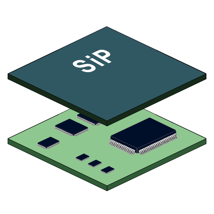
System-in-Package (SiP): SiP integrates multiple active components (like processors, memory chips), passive components, and various functional devices (such as MEMS, biochips, sensors) into a single package. Advances in 3D stacking technology have further propelled SiP towards higher integration and more complex functionalities.
Source: By Verdel - Own work, CC BY-SA 4.0) Fan-Out Wafer-Level Packaging (FoWLP): FoWLP embeds a single die into an Epoxy Mold Compound (EMC) and creates RDLs on the die and its surrounding area, thereby fanning out the I/O pins beyond the die's area. This technology offers higher I/O density, smaller package size, and improved thermal and electrical performance, and is considered a low-cost alternative to silicon interposer 2.5D/3D packaging.

Source:By 思考的苇丛 ) CoWoS (Chip-on-Wafer-on-Substrate - TSMC): CoWoS is a 2.5D interposer technology developed by TSMC. It places multiple dies (such as logic chips and High-Bandwidth Memory, HBM) side-by-side on a silicon interposer with TSVs, which is then packaged onto a substrate. CoWoS technology enables extremely high bandwidth and excellent integration, and is widely used in high-performance computing and AI chips.

SoIC (System-on-Integrated-Chips - TSMC): SoIC is a front-end 3D stacking technology introduced by TSMC, which uses direct copper-to-copper (Cu-to-Cu) hybrid bonding to achieve ultra-high-density vertical interconnects. SoIC can heterogeneously integrate chips of different sizes, functions, and process nodes, with bonding pitches reaching the sub-10-micron level, resulting in superior performance, lower power consumption, and smaller form factors. Companies like NVIDIA, AMD, and Apple have announced their adoption of SoIC technology.

Intel's Foveros and EMIB: Foveros is Intel's 3D die stacking technology, typically using an active interposer and micro-bumps for connection. Its derivative, Foveros Direct, uses copper-to-copper direct bonding. EMIB (Embedded Multi-die Interconnect Bridge) is a 2.5D solution that uses small, localized bridge dies to achieve high-density die-to-die interconnects, avoiding the cost and thermal limitations of large silicon interposers.
Samsung's X-Cube and I-Cube: X-Cube is Samsung's 3D IC packaging technology, which includes both micro-bump and hybrid copper bonding solutions. I-Cube is its 2.5D interposer solution.
Current Development Trends:
Advanced packaging technology is developing in several main directions:
Continuously Increasing Integration Density and Functionality: Integrating more and more complex functions within a single package is a primary goal.
Miniaturization and Thinning: The demand for thinner and smaller packages continues, especially in mobile and wearable devices.
Heterogeneous Integration: Integrating chiplets from different process nodes, with different functions, and even from different vendors into the same package has become a mainstream trend. This provides greater flexibility in system design, allowing for the selection of the most optimal process technology for different functional blocks.
Pursuit of Higher Bandwidth, Lower Latency, and Better Power Efficiency: This is key to meeting the demands of high-performance applications like AI and HPC.
Focus on the Reliability of High-Density Interconnects: As the pitch of micro-bumps, TSVs, and hybrid bonds continues to shrink, ensuring the long-term reliability of these fine interconnect structures under complex stress environments has become a research focus.
Popularization of the Chiplet Architecture: Chiplets have become the fundamental building blocks of advanced packaging, driving innovation in packaging technology.
A noteworthy trend is the "democratization" of packaging technology brought about by the rise of chiplets. In the past, designing a complex SoC required huge investment and integration capabilities. Today, the modular design of chiplets allows different manufacturers to focus on developing specific-function chiplets, which are then integrated through advanced 2.5D/3D packaging platforms. This model lowers the barrier to entry for high-performance chip design, enabling more small businesses or suppliers focused on specific IPs to participate in the construction of complex systems, thereby stimulating broader innovation. For example, Intel's EMIB technology allows customers to integrate dies from different foundries in the same package.
Another important development is the convergence of front-end processes and back-end packaging technologies. Taking TSMC's SoIC as an example, it is defined as a "front-end" 3D stacking technology that utilizes fab-level processes for direct copper-to-copper bonding, achieving ultra-high-density interconnects with pitches far smaller than traditional packaging bumps. The bump pitch of traditional back-end packaging is typically in the tens of microns, while SoIC's bonding pitch has entered the sub-10-micron range and is expected to shrink further. This direct bonding technology, such as copper-to-copper hybrid bonding, is usually performed at the wafer-level or die-to-wafer level and requires advanced lithography, etching, and bonding capabilities typically associated with front-end manufacturing. This means that achieving the interconnect density and performance of next-generation 3D packaging requires closer co-design and joint development among chip designers, foundries, and packaging houses, or for foundries to expand their services into areas traditionally belonging to packaging.
The following table summarizes the major advanced 3D/2.5D packaging technologies:
Table 1: Comparison Overview of Advanced 3D/2.5D Packaging Technologies
Technology Type | Key Structural Features | Primary Application Areas | Key Advantages | Major Thermal/Reliability Considerations |
TSV-based 3D IC | Vertically stacked dies, TSV interconnects, micro-bump bonding | HBM, sensors, some logic-memory stacks | Extremely high density, shortest interconnects, low power | Inter-layer thermal dissipation difficulty, TSV stress, TSV electromigration, stacking stress |
CoWoS (TSMC) | 2.5D, silicon interposer (with TSVs), micro-bumps connecting logic and HBM, then packaged on a substrate | HPC, AI accelerators, high-end FPGAs, network processors | Extremely high bandwidth, heterogeneous integration capability, mature ecosystem | Interposer heat dissipation, TIM challenges, substrate warpage, large package stress |
SoIC (TSMC) | 3D, direct Cu-to-Cu hybrid bonding, ultra-fine pitch (sub-10µm), bumpless, Wafer-on-Wafer (WoW) or Chip-on-Wafer (CoW) | High-performance logic, memory stacking, chiplet integration | Extremely high interconnect density, low electrical loss, small form factor, heterogeneous integration flexibility | Inter-layer heat dissipation, alignment and stress of hybrid bonding, thermal properties of thinned wafers |
Foveros/EMIB (Intel) | Foveros: 3D die stacking (active interposer/micro-bumps/direct bonding); EMIB: 2.5D local bridge die interconnect | CPU, GPU, AI chips, heterogeneous integration systems | Foveros: High-density stacking; EMIB: Modularity, cost-effectiveness | Foveros: Stack heat dissipation, power density; EMIB: Thermal interaction and stress between bridge die and main chip |
FoWLP | Die embedded in mold compound, RDL fanned out beyond die periphery, no interposer | Mobile communications, consumer electronics, IoT, power management | Low cost, thin profile, good electrical/thermal performance (vs. traditional WLP) | Thermal conductivity of mold compound, RDL stress, warpage control |
X-Cube/I-Cube (Samsung) | X-Cube: 3D die stacking (micro-bumps/hybrid copper bonding); I-Cube: 2.5D silicon interposer | HBM, mobile APs, server CPUs | X-Cube: High bandwidth, low power; I-Cube: Mature technology | X-Cube: Stack heat dissipation, hybrid bonding reliability; I-Cube: Interposer heat dissipation |
Driving Forces: The Urgent Demands of AI, HPC, and 5G in the "More than Moore" Era
The rapid development of advanced 3D packaging technology is not accidental but the result of multiple converging factors. The most fundamental driver is the slowdown of traditional Moore's Law. For decades, the semiconductor industry followed the guidance of Moore's Law, which states that the number of transistors on an integrated circuit doubles approximately every 18 to 24 months, leading to continuous performance improvements and cost reductions. However, as transistor sizes approach the atomic level, further scaling faces immense physical challenges and economic cost pressures. Against this backdrop, the concept of "More than Moore" emerged, and advanced packaging technology, especially 3D integration, has become a key pathway to continue the performance growth curve and achieve higher system integration.
Simultaneously, a series of emerging applications have placed unprecedentedly stringent demands on chip performance, power consumption, and size, further accelerating the adoption of advanced packaging technologies:
Artificial Intelligence (AI) and Machine Learning (ML): AI and ML applications, especially deep learning models, require large-scale parallel computing and have extremely high demands for memory bandwidth and latency. 3D integration technology, particularly the stacking of High-Bandwidth Memory (HBM) with logic chips, can significantly increase data transfer rates and reduce latency, thereby meeting the massive data throughput requirements of AI computing.
High-Performance Computing (HPC): The demands in the HPC field are similar to those of AI, also pursuing ultimate computing power and high-speed data exchange. Advanced packaging provides strong support for HPC systems through high-density integration and optimized interconnect solutions.
5G/6G Communications: The new generation of communication technologies requires smaller device sizes, higher operating frequencies, and the integration of more diverse components (such as RF, analog, and digital circuits). Advanced packaging technologies like SiP and FoWLP can achieve high integration of these complex functions in a compact space.
Automotive Electronics, Internet of Things (IoT), Edge Computing, Wearable Devices: These application scenarios have strong demands for chip miniaturization, power efficiency, and the integration of other functions like sensors. Advanced packaging technology can meet these diverse needs, driving the development of related industries.
Core Advantages of 3D/2.5D Integration:
Compared to traditional 2D planar packaging, 3D/2.5D integration technology offers several significant advantages:
Shorter Interconnect Lengths: Through vertical stacking or close side-by-side placement, the signal transmission paths between chips are greatly shortened, which reduces signal delay and power consumption while increasing data transfer bandwidth.
Smaller Footprint/Package Size: Vertical stacking significantly reduces the area occupied by chips on the Printed Circuit Board (PCB), making end products lighter, thinner, and smaller.
Enabling Heterogeneous Integration: This is one of the most attractive advantages of 3D/2.5D packaging. It allows chips from different process nodes, with different functions (such as logic, memory, sensors, RF), and even from different manufacturers to be integrated into the same package, achieving system-level optimal design.
The Worsening Thermal Dilemma in Vertical Integration Architectures
As advanced 3D packaging technology integrates an increasing number of transistors and functional units into ever-shrinking spaces, thermal management has become a critical bottleneck hindering further performance improvements and ensuring reliability. This "thermal nightmare" stems from the cumulative effect of multiple physical factors.
The Physics of Heat Generation: Soaring Power Density and Proliferating Hot Spots
The essence of 3D integration architecture is to vertically stack multiple active dies or package them in a high-density 2.5D configuration, which inevitably leads to a sharp increase in power consumption per unit volume, i.e., a significant increase in power density. For example, in some 2.5D packaging platforms, the heat flux has exceeded 100W/cm2, and the power density of microprocessors has climbed from about 40W/cm2 to around 100W/cm2. Furthermore, some advanced cooling technology demonstrations are targeting an average power density of 350W/cm2 and local hot spot power densities exceeding 2kW/cm2. In the future, power density is expected to continue to rise, with some applications potentially reaching levels of 500W/cm2.
At the same time, the nature of heterogeneous integration means that the power consumption of different chips or different functional blocks within the same chip can vary greatly. This leads to the formation of "hot spots" in local areas where the temperature is much higher than the average chip temperature. These hot spots are like dormant volcanoes, posing a serious threat to the performance and reliability of the chip. For example, in a structure where memory is stacked on logic (MoL) or logic on memory (LoM), the location of the hot spot will shift accordingly.
To make matters worse, silicon wafers are often thinned to facilitate 3D stacking and TSV formation. However, the thermal conductivity of a thinned silicon wafer decreases as its thickness is reduced. This means that the chip's own lateral heat conduction capability is weakened, making it more difficult for heat to spread out from hot spot areas, further exacerbating the thermal resistance within the chip and hindering effective heat dissipation.
This combination of rising power density, reduced thermal conductivity due to silicon wafer thinning, and increasingly complex thermal paths (as detailed later) creates a highly challenging thermal situation. The large amount of heat generated by high power density is trapped within thinned chips with poor thermal conductivity and struggles to be effectively conducted to external cooling systems through increasingly complex vertical paths. This synergistic negative effect makes the hot spot problem more prominent, with higher temperatures that are more difficult to cool.
Navigating Complex Thermal Paths and Managing Thermal Crosstalk
In a 3D package structure, heat must travel a long and tortuous path from its source to its eventual dissipation into the external environment. This path includes multiple layers of silicon chips, Thermal Interface Materials (TIMs), interposers, substrates, etc., each with different thermal conductivities, and with thermal resistance at each material interface. This complex thermal conduction path is often inefficient and prone to creating thermal bottlenecks. For example, in a 2.5D package, heat may need to pass through TIM1, an interposer, and TIM2 before reaching the heat sink. In a 3D stack, all chip layers share a common, longer thermal path, making the thermal gradient steeper.
Each material interface, such as between the die and TIM, TIM and heat sink, or die and interposer, introduces Thermal Interface Resistance (TIR). The presence of TIR impedes the smooth flow of heat. In a 3D stacked structure with numerous interfaces, the cumulative effect of TIR can be very significant, becoming one of the main limiting factors for overall thermal performance.
A more intractable problem is thermal crosstalk. In a highly integrated heterogeneous system, the heat generated by one chip or die can significantly affect the temperature and performance of adjacent or vertically stacked components. For example, in 2.5D packaging, to ensure signal and power integrity, logic chips and HBM are often placed very close to each other (e.g., within 500 microns), which makes it easy for the heat generated by the logic chip to be conducted to the more temperature-sensitive HBM, leading to increased leakage current, performance degradation, and even a shortened lifespan for the HBM. If not properly managed, this thermal crosstalk effect can negate the performance or reliability advantages brought by heterogeneous integration. This means that when planning chiplet layouts, it is necessary to consider not only electrical connections but also thermal isolation strategies, such as strategically increasing the spacing between chiplets or using low-thermal-conductivity molding compounds as thermal barriers.
Joule Heating Contribution from Interconnects, TSVs, and Power Delivery Networks (PDNs)
In addition to the active power consumption of the chip itself, Joule heating (I2R loss) generated when current flows through conductors is a non-negligible heat source in 3D packaging, especially in interconnect structures, TSVs, and Power Delivery Networks (PDNs).
As interconnect line widths shrink and current densities increase, the Joule heating effect in RDLs, micro-bumps, and internal chip wiring becomes increasingly significant. High current density flowing through TSVs also generates considerable Joule heat, which not only increases the overall thermal load but can also form local hot spots within or around the TSVs.
The efficiency of the PDN also directly affects heat generation. The resistance in the PDN, including the TSVs used for power delivery, generates Joule heat as current flows through it. More importantly, Joule heating is a problem coupled with temperature. The resistivity of a conductor increases with temperature, which means that the generation of Joule heat leads to a local temperature rise, which in turn further increases the conductor's resistance, generating more Joule heat at the same current. If not properly controlled, this positive feedback effect can even trigger thermal runaway. Therefore, accurate electro-thermal co-simulation is crucial for predicting and managing temperatures in advanced packaging, as purely thermal simulations may underestimate the impact of Joule heating.
The following table summarizes the major thermal challenges in advanced 3D packaging:
Table 2: Major Thermal Challenges in Advanced 3D Packaging
Thermal Challenge | Description | Key Contributing Factors in 3D Architectures | Typical Reported Magnitudes/Impacts |
High Power Density | Significant increase in power consumption per unit volume, leading to massive overall heat generation. | Vertical stacking of multiple active dies or high-density 2.5D arrangement. | >100 W/cm², hot spots can reach >2 kW/cm², future may reach 500 W/cm². |
Localized Hot Spots | Formation of local high-temperature areas within the package, with temperatures far exceeding the average, due to heterogeneous integration and power differences in functional blocks. | Uneven power consumption of different chips/functional blocks, thinned silicon wafers reducing lateral heat conduction. | Hot spot temperatures can be tens of degrees higher than average chip temperature, hot spot power density can reach 1000 W/cm². |
Complex/High-Impedance Thermal Path | Heat must travel through multiple layers of materials with different thermal conductivities and interfaces, forming a tortuous and high-thermal-resistance path. | Multi-layer stack structure (silicon, TIM, interposer, substrate), with Thermal Interface Resistance (TIR) at each interface. | Significant increase in total thermal resistance, limiting heat dissipation efficiency. |
Thermal Crosstalk | Heat generated by one chip or die affects the temperature and performance of adjacent or stacked components. | High-density packaging, close proximity of heterogeneous components (e.g., logic chip and HBM spacing <500 µm). | Can lead to increased leakage current and performance degradation in sensitive components (e.g., memory). |
Joule Heating in Interconnects/TSVs | I2R heat generated as current flows through interconnect structures like RDLs, micro-bumps, and TSVs, becoming an additional heat source. | Shrinking interconnect dimensions, increasing current density, temperature dependence of material resistivity. | Joule heating contribution is increasingly significant, potentially leading to local overheating or even thermal runaway. |
Reliability Under Thermal Stress: Thermomechanical and Electrical Degradation
While pursuing ultimate performance, the complex structure and harsh thermal environment of advanced 3D packaging also pose unprecedented challenges to the long-term reliability of the package. High temperatures and temperature cycling not only accelerate material aging but also induce significant thermomechanical stress, leading to various structural failures. Furthermore, electrical degradation mechanisms like electromigration become more active at high temperatures and high current densities. These factors, acting in concert, can lead to unstable package performance, shortened lifespan, and even catastrophic failure.
Material Degradation Mechanisms: Aging of Dielectrics, Thermal Interface Materials, and Solder Interconnects
Under continuous high temperatures or repeated temperature fluctuations, the various materials that constitute a 3D package gradually undergo changes in their physical and chemical properties, a process known as material aging, which affects their function and the overall reliability of the package.
Dielectric Material Aging: The low-k (low dielectric constant) and ultra-low-k materials, such as SiOCH and SiOx, widely used in the Back-End-of-Line (BEOL) and interposers, are prone to degradation under thermal stress and temperature cycling. Their degradation mechanisms include chemical bond breaking and recombination (e.g., condensation of silanol groups in SiOx), degradation of pendant groups (e.g., breaking of alkyl chains in SiOCH), changes in material porosity, and the evolution of internal defects. These microstructural changes directly affect the macroscopic electrical properties of the dielectric materials, such as dielectric constant drift and increased insertion loss, which in turn affect signal integrity and high-speed performance.
Thermal Interface Material (TIM) Degradation: As a critical material for filling the microscopic air gaps between the chip and the heat sink to reduce contact thermal resistance, the long-term stability of TIMs is crucial. However, common TIM materials, such as thermal grease, thermal gels, thermal pads, and phase change materials, can experience phenomena like "pump-out" (material being squeezed out from the interface), "dry-out" (evaporation or separation of liquid components), "voiding," "cracking," and "loss of adhesion" to contact surfaces under long-term high-temperature operation or temperature cycling. These degradations lead to a decrease in the effective thermal conductivity of the TIM and an increase in interface thermal resistance, thereby weakening the heat dissipation effect and causing the chip temperature to rise. Even better-performing gel-type TIMs can have issues with expansion during BGA reflow or Surface Mount Technology (SMT) assembly processes.
Solder Bump/Interconnect Degradation: Solder joints like micro-bumps and BGA balls are the primary electrical and mechanical connection structures in 3D packaging. Under the dual effects of temperature cycling and high current density, these solder joints are prone to degradation phenomena such as fatigue, creep, excessive growth of Intermetallic Compounds (IMCs), and void formation. High temperatures accelerate the growth rate of IMCs, and overly thick IMC layers are typically brittle and prone to cracking. At the same time, high temperatures and high current densities also promote the nucleation and growth of voids within the solder joints, which can eventually lead to increased resistance or even open circuits.
Mechanical Stress and Failure: Warpage, Cracking, Delamination, and Bump Fatigue
The mismatch in the Coefficient of Thermal Expansion (CTE) between different materials is the main source of thermomechanical stress in 3D packaging. When the package undergoes temperature changes (such as cooling down during manufacturing or power cycling during actual operation), the CTE mismatch causes the internal components to expand or contract to different degrees, leading to stress concentration and potentially a series of mechanical failure modes.
Package/Die Warpage: CTE mismatch can cause the entire package or individual dies to bend and deform, a phenomenon known as warpage. Severe warpage not only affects subsequent assembly processes (like heat sink installation) but can also lead to solder joint connection failures (e.g., open BGA balls) and poor TIM contact. Studies have shown that substrate thickness, material selection (such as low-CTE substrates and underfills), and the size ratio of the chip to the package all affect the degree of warpage.
Cracking and Delamination: Once the long-term accumulated thermomechanical stress exceeds the fracture strength of a material or the bonding strength of an interface, it can lead to cracking or delamination. Cracking can occur in the die itself, the interposer, dielectric layers, underfill, etc. Delamination often occurs at the interface between different materials, such as the interface between a TSV and the surrounding dielectric layer, or the interface between a die and the underfill.
Solder Joint Fatigue / Bump Fatigue: Under repeated temperature cycling, solder bumps experience cyclic loading of stress and strain, which induces fatigue damage. This usually manifests as the initiation and propagation of fatigue cracks, eventually leading to the electrical disconnection of the solder joint. This is a typical creep-fatigue interaction mechanism. The use of underfill can effectively distribute stress and improve the fatigue life of solder joints.
Electromigration: A Persistent Threat to Interconnect Integrity, Especially in TSVs
Electromigration (EM) is the phenomenon where metal atoms in a conductor migrate due to the impact of a strong electric field and electron flow. Under the combined effects of high current density, high temperature gradients, and mechanical stress, the problem of electromigration is particularly prominent. Electromigration can lead to the formation of voids in certain areas of a metal conductor due to atomic depletion, causing open circuits, and the formation of hillocks in other areas due to atomic accumulation, which can cause short circuits.
Electromigration in TSVs: Due to their special geometric structure and operating environment, TSVs are a high-risk area for electromigration. First, TSVs may carry high current densities. Second, there is often a significant size mismatch between TSVs and their top and bottom landing pads or wiring, which can easily cause current crowding and stress concentration. More importantly, the thermomechanical stress in TSVs caused by CTE mismatch interacts with electromigration, further accelerating the failure process. Studies have shown that the stress gradient around a TSV has a significant impact on its electromigration lifetime.
Electromigration in Other Interconnect Structures: Interconnect structures like micro-bumps and RDLs also face the challenge of electromigration under high current density and high operating temperatures. In solder bumps, current crowding accelerates IMC reactions and leads to thickening of the IMC at the anode end and the formation of voids and cracks at the cathode end. It also creates a temperature gradient that induces thermomigration. The combined effect of electromigration and thermomigration accelerates solder joint failure.
As the core components of 3D integration, the reliability of TSVs is crucial for the entire package. They not only bear huge thermomechanical stress due to the CTE mismatch between silicon and the filling metal (usually copper) but are also high-risk points for electromigration. This dual pressure makes TSVs a weak link in the reliability chain of 3D packaging. Therefore, the design of TSVs (such as geometry, material selection) and their manufacturing process (such as interface quality control) are of decisive significance for ensuring the long-term stable operation of 3D packages.
Impact on Performance Stability: Reduced Timing Margins and Increased Leakage Current
High temperatures and hot spots not only directly threaten the physical integrity of the package but also have a significant negative impact on the electrical performance and stability of the chip.
Impact of Temperature on Component/Interconnect Delay: The carrier mobility of semiconductor devices and the resistivity of interconnect wires are both sensitive to temperature. An increase in temperature leads to a decrease in carrier mobility and an increase in resistivity, which in turn increases logic gate delay and interconnect line RC delay. This increase in delay compresses the circuit's timing margin and, in severe cases, can lead to timing failures, forcing designers to adopt more conservative timing designs, thereby sacrificing some performance.
Increased Leakage Current: The leakage current of a chip (including sub-threshold leakage and gate leakage) is exponentially sensitive to temperature. An increase in operating temperature, especially the presence of local hot spots, leads to a sharp increase in leakage current. The increase in leakage current not only increases the static power consumption of the chip but, more importantly, also generates heat itself, further pushing up the chip temperature. If this "temperature-leakage current" positive feedback loop cannot be effectively controlled, it can lead to consequences ranging from excessive power consumption and performance degradation to thermal runaway and permanent damage. This thermal feedback loop not only risks thermal runaway but also continuously degrades performance by increasing delay and reducing timing margins, making stable operation a dynamically changing target.
Impact of Hot Spots on Performance and Stability: Local hot spots can cause severe performance degradation in the affected area, reduce local timing margins, and contribute disproportionately to the overall leakage current. Since traditional surface cooling methods may not be able to effectively cool hot spots buried deep within a 3D structure, more targeted thermal management strategies are needed.
These thermally induced degradation mechanisms often do not occur in isolation but are intertwined and mutually reinforcing. For example, high temperature accelerates the aging of TIMs, and degraded TIMs lead to higher chip temperatures, which in turn exacerbates CTE mismatch stress, potentially causing warpage or cracking, while also promoting electromigration in interconnect structures. This complex coupling effect makes the reliability prediction and mitigation measures for 3D packaging extremely challenging, requiring a comprehensive consideration of the interaction of multiple physical fields.
The following table systematically records the major reliability failure mechanisms in 3D packaging under thermal stress:
Table 3: Major Reliability Failure Mechanisms in 3D Packaging Under Thermal Stress
Failure Mechanism | Physical Process Description | Affected Components/Materials in 3D Stack | Primary Stress Sources | Typical Manifestation/Consequence |
Dielectric Material Aging (SiOCH/SiOx) | Chemical bond changes, pendant group degradation, porosity changes, defect evolution under thermal stress. | BEOL dielectric layers, interposer dielectrics | High-temperature soak, temperature cycling | Dielectric constant drift, increased insertion loss, decreased signal integrity. |
TIM Degradation (Pump-out/Dry-out) | Material squeezed out from interface, liquid component evaporation/separation, void formation, cracking, loss of adhesion. | TIM1 (Die-Lid/Spreader), TIM2 (Lid/Spreader-Heat Sink) | High-temperature soak, temperature cycling, mechanical stress | Increased interface thermal resistance, decreased heat dissipation efficiency, increased chip temperature. |
Solder Joint Fatigue/Creep (BGA/Micro-bumps) | Crack initiation and propagation due to cyclic stress-strain loading under temperature cycling; permanent deformation under sustained stress at high temperature. | BGA balls, micro-bumps, C4 bumps | Temperature cycling, CTE mismatch, high current density (accelerates creep) | Increased resistance, electrical open, mechanical connection failure. |
Package/Die Warpage | Bending deformation of the package or die during temperature changes due to CTE mismatch of different materials. | Entire package, die, substrate, interposer | Temperature changes during manufacturing, temperature cycling in operation, CTE mismatch | Assembly difficulty, open solder joints, poor TIM contact, decreased reliability. |
Interface Delamination (TSV/Underfill) | Separation of different material layers when stress exceeds interface bonding strength. | TSV-dielectric interface, die-underfill interface, inter-layer dielectric interface | Temperature cycling, CTE mismatch, manufacturing defects | Electrical connection failure, interruption of thermal path, structural integrity failure. |
Die/Interposer Cracking | Crack formation when stress exceeds the material's fracture strength. | Silicon die, silicon/glass interposer, dielectric layers | Thermomechanical stress, CTE mismatch, manufacturing defects | Chip functional failure, electrical open. |
Electromigration in TSVs | Migration of TSV fill metal (e.g., copper) atoms along the electron flow direction under high current density and temperature, forming voids or hillocks. | TSV fill metal, TSV-pad/wiring interface | High current density, high temperature, thermomechanical stress, geometric mismatch | Increased TSV resistance, open or short circuit, affecting vertical interconnects in 3D stack. |
Electromigration in Bumps/RDLs | Similar atomic migration phenomenon in micro-bumps and RDLs under high current density and temperature. | Micro-bumps, RDL traces | High current density, high temperature, current crowding | Increased interconnect resistance, open or short circuit. |
Thermal Management Innovations: Current Strategies and Emerging Solutions
Facing the increasingly severe thermal challenges of 3D packaging, academia and industry are actively exploring and developing various innovative thermal management strategies. These strategies range from breakthroughs in materials science to the integration of advanced cooling systems, all aimed at effectively removing heat from high-power-density packages to ensure their performance and reliability.
Thermal Interface Materials (TIMs): Advancements, Performance Limitations, and Degradation Challenges
Thermal Interface Materials (TIMs) play a crucial role in the thermal management of electronic packages. They are used to fill the microscopic air gaps that exist between the chip, heat spreader, and heat sink, thereby reducing contact thermal resistance and providing a low-impedance path for heat conduction. In a typical package structure, there is TIM1 (located between the die and the heat spreader/lid) and TIM2 (located between the heat spreader/lid and the external heat sink).
Currently, there are various types of TIMs on the market, including thermal greases, thermal gels, thermal pads, phase change materials (PCMs), solder-based TIMs, liquid metals, and emerging nanocomposites. When selecting a TIM, it is necessary to consider its bulk thermal conductivity, the Bond Line Thickness (BLT) after application, contact thermal resistance, and long-term reliability under temperature cycling and high-temperature environments.
Despite continuous advancements in TIM technology, its performance and reliability still face challenges. As mentioned earlier, TIM materials are prone to degradation phenomena such as pump-out, dry-out, voiding, and cracking under high temperatures and temperature cycling, leading to an increase in interface thermal resistance over time. These problems are more common with non-bonding TIMs (like thermal grease). Although solder-based TIMs have excellent initial thermal performance, they are prone to creep at high temperatures. Ensuring the quality of TIMs under an integrated heat spreader often requires non-destructive testing methods like Scanning Acoustic Tomography (SAT) for monitoring.
To overcome these limitations, researchers are dedicated to developing new types of TIMs. For example, nanocomposite TIMs, such as Nano-TIMs made from a composite of silver-coated nanofiber networks and an indium matrix, have shown low thermal resistance comparable to pure indium while having superior mechanical properties. Additionally, self-assembled boron arsenide composites show application potential due to their high thermal conductivity and good mechanical compliance. Carbon nanotube (CNT) array TIMs are also considered promising future materials due to their excellent thermal and mechanical properties, but their bonding technology needs further development.
Heat Spreaders: From Traditional Materials to Advanced Composites (e.g., Diamond, Boron Nitride)
The main function of a heat spreader is to spread the concentrated heat from a small die or local hot spots over a larger area, thereby reducing the heat flux transferred to TIM2 and the external heat sink and improving overall heat dissipation efficiency.
Traditional heat spreader materials are mainly copper and aluminum, due to their high thermal conductivity and good processability. Many packages incorporate an Integrated Heat Spreader (IHS).
As the demand for thermal performance increases, research has shifted towards advanced materials and composites with higher thermal conductivity:
Hexagonal Boron Nitride (hBN): hBN has high thermal conductivity and excellent electrical insulation properties, making it an ideal material for heat spreaders that can both effectively dissipate heat and maintain electrical isolation. hBN nanosheets can be prepared by methods like liquid-phase exfoliation and made into flexible, uniform hBN film heat spreaders.
Diamond: Diamond is currently known to have the highest thermal conductivity of any material. Polycrystalline Diamond (PCD) heat spreaders and diamond matrix scaffolds integrated into the Back-End-of-Line (BEOL) have shown great potential in lateral heat spreading and reducing hot spot temperatures. The thermal conductivity of PCD can reach 500−1800W/mK.
Graphene-Carbon Nanotube (G-CNT) Hybrid Heat Spreaders/Sinks: This composite material combines the excellent lateral thermal conductivity of 2D graphene with the enhanced convective/vertical heat transfer capabilities of 1D carbon nanotubes, promising efficient multi-dimensional heat dissipation.
Glass Interposers with Through-Glass Vias (TGVs): Glass materials have good thermal stability and a low CTE close to that of silicon. Integrating TGVs into an interposer can significantly increase local thermal conductivity, for example, from about 1.2W/mK for pure glass to about 94W/mK, providing a new way to manage thermal challenges in advanced electronic packaging.
The optimization strategy for heat spreaders involves material selection, geometric design, and integration with TIMs and cooling solutions. Additive Manufacturing (AM) technology has opened up new possibilities for manufacturing heat spreaders with complex geometries.
Embedded and Advanced Cooling Technologies
As power densities continue to climb, traditional air cooling and indirect liquid cooling solutions are becoming inadequate. To cope with extreme heat dissipation demands, a series of more direct and efficient embedded and advanced cooling technologies have emerged.
Microfluidics and On-Chip Liquid Cooling:
Concept: The core idea of this technology is to introduce a liquid coolant directly into or between chips by etching microchannels or microgaps in the silicon die or interposer, or by utilizing the gaps between stacked dies, allowing the coolant to flow through hot spot areas and directly carry away heat.
Types: This includes single-phase liquid cooling and phase-change liquid cooling (which utilizes the large amount of latent heat absorbed during liquid boiling for higher heat transfer efficiency). Dielectric coolants are usually chosen to avoid electrical issues.
Performance: Microfluidic cooling can handle extremely high power densities, for example, it has been demonstrated to cool an average power density of 350W/cm2 and hot spots exceeding 2kW/cm2, as well as a volumetric heat flux of up to 2870W/cm3, and can significantly reduce chip temperatures.
Manufacturing and Integration Challenges: Despite its promising prospects, the implementation of microfluidic cooling faces many challenges, including complex manufacturing processes (such as Deep Reactive-Ion Etching, DRIE, and wafer bonding), integration with TSVs, fluid manifold design, pumping power consumption, reliability of fluid connections, cost, and scalability for mass production. Research institutions like IMEC are exploring the use of additively manufactured ceramic (e.g., SiC) coolers to address these challenges.
Immersion Cooling:
Concept: This involves completely immersing an entire electronic assembly or server in a dielectric liquid, using the liquid's convection and/or phase change to carry away heat from all surfaces.
Feasibility and Advantages: For high-density data center applications, immersion cooling has the potential for efficient heat dissipation and reduced fan energy consumption, and may improve system reliability by reducing oxidation and dust contamination.
Challenges: The main challenges include material compatibility (the dielectric liquid may affect the physical properties of the PCB, such as Young's modulus and glass transition temperature), liquid sealing, maintenance, cost, and the lack of extensive long-term reliability data.
Jet Impingement Cooling:
Concept: This involves directing a high-velocity fluid jet (liquid or gas) to impinge directly on a hot surface, utilizing the extremely high local heat transfer coefficient for cooling.
Effectiveness: It can achieve extremely high heat transfer coefficients, making it very suitable for targeted cooling of intense local hot spots. Studies have demonstrated heat transfer coefficients exceeding 250kW/m2K, capable of cooling heat fluxes up to 5500W/cm2.
Challenges: Cooling uniformity, fluid management, nozzle clogging, surface erosion, integration complexity, scalability, and cost are the main obstacles. Additive manufacturing technology is being used to create complex jet impingement cooler structures.
Miniature and Flat Heat Pipes:
Concept: A heat pipe is a passive two-phase heat transfer device that efficiently transfers heat using the evaporation and condensation of a working fluid within a sealed structure. Flat or miniature heat pipes can be embedded inside a PCB or package substrate to achieve efficient heat spreading.
Manufacturing and Performance: They can be manufactured using PCB fabrication processes or 3D printing technology. They can provide an equivalent thermal conductivity far higher than solid conductive materials, for example, it has been reported that their equivalent thermal conductivity can be more than seven times that of solid copper.
Challenges: The design of the capillary wick structure, selection of the working fluid, sealing, integration in small form factors, and the manufacturing complexity of embedded versions are the main challenges.
The Key Role of Thermal Through-Silicon Vias (TTSVs) and Thermal Collection Networks (TCNs)
In addition to the external or embedded cooling solutions mentioned above, optimizing the thermal conduction paths within the chip is also an important part of thermal management. Thermal Through-Silicon Vias (TTSVs) and Thermal Collection Networks (TCNs) are designed for this purpose.
Thermal Through-Silicon Vias (TTSVs): TTSVs are TSVs specifically designed for thermal conduction. They provide a low-thermal-resistance vertical path for dies or local hot spots buried deep in a 3D stack, effectively conducting heat to the upper heat spreader or heat sink.
Thermal Collection Networks (TCNs): TCNs are metal trace networks designed in the Back-End-of-Line (BEOL) layers of a chip to collect heat from distributed heat sources (like logic circuits) and channel it to TTSVs, which then conduct it away.
Effectiveness and Impact on Thermal Budget: Studies have shown that the combination of TTSVs and TCNs can significantly reduce the maximum chip temperature and effectively remove heat from hot spot areas. For example, in one study, a 3D IC structure using TCNs and TTSVs improved the heat extraction efficiency from the hot spot area by 11% to 35% compared to a conventional solution.
Challenges: The implementation of TTSVs and TCNs also faces some challenges, including area overhead, CTE mismatch issues with the surrounding silicon or dielectric materials, the risk of causing large-area overheating if not designed properly, and increased manufacturing complexity.
Optimization: The layout of TTSVs (position, density), their diameter, pitch, aspect ratio, and filling material (e.g., comparing copper with carbon nanotubes) are all key design parameters that affect their thermal performance and need to be carefully optimized.
Novel Thermal Management Materials: Carbon-Based Nanomaterials and Diamond Substrates/Matrix Scaffolds
Advances in materials science have provided new ideas for solving the thermal challenges of 3D packaging. Among them, carbon-based nanomaterials and diamond materials have attracted much attention for their excellent thermal properties.
Carbon-Based Nanomaterials (CNTs, Graphene):
Properties: Carbon nanotubes (CNTs) and graphene both have extremely high intrinsic thermal conductivity and excellent mechanical strength. Due to their one-dimensional structure, CNTs are very suitable for vertical heat transfer, while 2D graphene excels at in-plane lateral heat spreading.
Applications:
Nanocomposite TIMs: Adding CNTs or graphene as fillers to a traditional TIM matrix can significantly increase its thermal conductivity.
CNT-based TSVs: Compared to traditional copper TSVs, CNT-filled TSVs have a lower CTE, which better matches the thermal expansion of silicon, and they exhibit superior electromigration resistance at high current densities.
Graphene-CNT Hybrid Heat Spreaders/Sinks: Combining the advantages of both to achieve efficient multi-dimensional heat dissipation.
CNT Array TIMs: Using vertically aligned CNT arrays as TIMs promises to achieve extremely low interface thermal resistance.
Challenges: Despite their promising prospects, the practical application of carbon-based nanomaterials still faces challenges such as high interface thermal resistance, difficulty in large-scale controlled preparation, high cost, and integration compatibility with standard CMOS processes.
Diamond Substrates/Matrix Scaffolds:
Properties: Diamond has the highest room-temperature thermal conductivity of any known material (polycrystalline diamond, PCD, can reach 500−1800W/mK), along with good electrical insulation (low dielectric constant) and a low Thermal Boundary Resistance (TBR) with silicon.
Applications: Studies have shown that two layers of PCD matrix scaffolds can be grown compatibly within the BEOL process to replace copper thermal vias for vertical heat conduction. At the same time, the PCD layer can also serve as an efficient lateral heat spreading layer integrated into the Interlayer Dielectric (ILD).
Performance: Experiments have demonstrated that integrating diamond matrix scaffolds can significantly reduce hot spot temperatures in 3D ICs and make the temperature distribution more uniform.
Manufacturing and Challenges: Low-temperature Chemical Vapor Deposition (CVD) growth of high-quality PCD, polishing and planarization of PCD films, integration with existing BEOL processes, and management of residual stress are the main manufacturing challenges.
As can be seen from the diverse solutions above, there is no "silver bullet" for the thermal management of 3D packaging. Each technology has its specific application scenarios, advantages, and limitations. For example, jet impingement cooling may be suitable for dealing with extreme local hot spots, while immersion cooling is more appropriate for the overall heat dissipation of large systems, and embedded microfluidics focuses on direct die cooling. Therefore, future thermal design will likely need to adopt a "multi-modal" or "toolbox" approach, flexibly combining and customizing multiple thermal management technologies based on specific application requirements, power levels, cost constraints, and form factor considerations. This also means that system-level co-optimization and design will become even more important.
At the same time, in-depth research into new materials like carbon nanomaterials and diamond indicates that breakthroughs in materials science are playing a role just as important as innovations in cooling hardware engineering in the field of thermal management. The synthesis, processing, and large-scale integration capabilities of these advanced materials will be key factors determining the upper limits of future thermal management technology. However, although efficient cooling solutions like microfluidics and embedded heat pipes have achieved encouraging results in the laboratory, their path to High-Volume Manufacturing (HVM) is still fraught with challenges related to cost, complexity, reliability, and integration with existing semiconductor manufacturing flows. Additive manufacturing technology offers some new possibilities in this regard, but its own large-scale application and material limitations in the packaging field have yet to be overcome. How to cost-effectively and reliably mass-produce these complex cooling solutions is one of the core obstacles to unlocking the full potential of 3D ICs.
The following table provides a comparative analysis of thermal management solutions for advanced 3D ICs:
Table 4: Comparative Analysis of Thermal Management Solutions for Advanced 3D ICs
Solution Category | Specific Examples/Materials | Working Principle | Reported Effectiveness (e.g., Cooling Power Density, ΔT Reduction, k_eff) | Key Advantages | Key Challenges (Integration, Cost, HVM, Reliability) |
Advanced TIMs | Nanocomposite TIMs (e.g., Ag-nanofiber/In), Self-assembled Boron Arsenide composites, CNT array TIMs | Fills microscopic air gaps at interfaces, reduces contact thermal resistance, provides an efficient heat conduction path. | Nano-TIM thermal resistance 2.1 K·mm²/W. Boron Arsenide composite thermal conductivity 21 W/mK. | Significantly reduces interface thermal resistance, improves heat conduction efficiency. | Material stability, long-term reliability (pump-out, dry-out), cost, compatibility with different surfaces, manufacturability. |
Novel Heat Spreaders | Hexagonal Boron Nitride (hBN), Polycrystalline Diamond (PCD), Graphene-CNT hybrid materials, Glass interposers with TGVs | Uses high-thermal-conductivity materials to spread concentrated heat laterally over a larger area. | hBN effectively reduces hot spot temperature by ~20 °C. PCD thermal conductivity 500-1800 W/mK. Glass+TGV local thermal conductivity up to 94 W/mK. | Excellent thermal spreading capability, can reduce heat flux density, some materials also have electrical insulation. | Material cost (especially diamond), manufacturing process complexity, CTE matching with other package materials, mechanical strength. |
Microfluidics/On-Chip Liquid Cooling | Single/two-phase microchannel cooling, dielectric coolants | Flows coolant directly through microchannels/microgaps within or between chips to efficiently remove heat. | Can cool >350 W/cm², hot spots >2 kW/cm², volumetric heat flux 2870 W/cm³. | Extremely high heat dissipation efficiency, can directly cool hot spots. | Manufacturing complexity (etching, bonding), fluid manifold design, pumping power, sealing and leakage risk, long-term reliability, cost, HVM scalability. |
Immersion Cooling | Single/two-phase dielectric liquid immersion | Immerses the entire electronic system in a dielectric coolant, dissipating heat through natural/forced convection or phase change. | Suitable for high-density data centers, can significantly reduce cooling energy consumption. | Good overall heat dissipation, can reduce fan noise and power consumption. | Material compatibility (liquid's effect on PCB/components), liquid leakage and maintenance, system complexity, cost, lack of long-term reliability data. |
Jet Impingement Cooling | High-velocity liquid/gas jets | Impinges a high-velocity fluid directly onto a hot surface, using an extremely high local heat transfer coefficient to carry away heat. | Heat transfer coefficient can reach 250 kW/m²K, can cool 5500 W/cm² heat flux. | Targeted, high-efficiency cooling, suitable for extreme hot spots. | Cooling uniformity, fluid management, nozzle clogging/erosion, integration complexity, noise (gas jets), cost, scalability. |
Miniature/Flat Heat Pipes | Embedded flat heat pipes, 3D-printed heat pipes | Utilizes the evaporation-condensation cycle of a working fluid in a sealed cavity to transfer heat. | Equivalent thermal conductivity can be >7 times that of solid copper. 3D-printed FOHPFR thermal resistance reduced by 65.6%. | Passive, high-efficiency heat transfer, no additional power consumption. | Wick structure design, working fluid selection, sealing, difficulty of small-scale integration, manufacturing complexity of embedded versions. |
Thermal Vias (TTSV)/Thermal Collection Networks (TCN) | Copper-filled TTSVs, TCN metal networks in BEOL layers | TTSVs provide a vertical low-resistance thermal path, TCNs collect and guide heat to TTSVs. | Can significantly reduce maximum chip temperature, heat extraction efficiency 11-35%. | Removes heat directly from within the chip, highly targeted. | Chip area overhead, CTE mismatch, potential overheating risk, manufacturing complexity. |
Resilient Design: Methodologies and Tools for Thermally Robust 3D ICs
To address the severe thermal challenges in advanced 3D packaging and their profound impact on reliability, the industry is starting from the design source, developing a series of methodologies and tools aimed at enhancing thermal robustness. The core idea is to integrate thermal management and reliability considerations into the early stages of the design flow, achieving co-optimization of electrical, thermal, and mechanical multi-physics fields.
Design for Thermal Reliability (DfTR) Principles for 3D Architectures
Design for Thermal Reliability (DfTR) emphasizes the proactive inclusion of thermal and reliability factors at the beginning of the design process, rather than as a remedial measure in the later stages. This requires a comprehensive consideration and co-optimization of the chip's electrical performance, thermal behavior, and mechanical stress.
Key DfTR strategies include:
Material Selection: Carefully selecting materials with appropriate CTEs, high thermal conductivity, and good mechanical properties to minimize thermal mismatch stress and enhance the efficiency of heat transfer from the source to the heat sink. For example, choosing interposer materials with a CTE close to that of silicon, or using highly conductive TIMs and heat spreaders.
Structural Design: Optimizing the package geometry, the thickness of various functional layers, the layout and density of TSVs, and the routing paths of interconnects to effectively manage stress distribution and improve thermal paths. For example, using a reasonable TSV array arrangement to enhance vertical thermal conduction, or designing stress buffer structures.
Power Distribution Management: Designing an efficient Power Delivery Network (PDN) to minimize the generation of Joule heat and ensure a stable power supply, avoiding local power consumption increases due to excessive voltage drop.
Hot Spot Mitigation: Reducing peak temperatures through design measures (such as dispersing high-power units) or active management techniques (like Dynamic Voltage and Frequency Scaling, DVFS) to avoid local overheating.
This shift from passive response to active prediction and prevention is a major advancement in 3D IC design philosophy. Given the complexity and high redesign costs of 3D ICs, foreseeing and mitigating potential thermal issues during the architecture definition and layout planning stages is crucial for ensuring the final success of the product.
Thermal-Aware Floorplanning, Placement, and Routing Strategies
In the physical design stage, adopting thermal-aware floorplanning, placement, and routing strategies is crucial for optimizing the thermal characteristics of a 3D IC, reducing hot spots, and managing thermomechanical stress, while also balancing traditional design goals such as wirelength, performance, and area.
Specific techniques include:
Strategic Spacing Between Chips: In 2.5D or 3D chiplet integration, reasonably increasing the spacing between high-power chips can effectively reduce thermal crosstalk and stress concentration.
Layout of High-Power Modules: Placing high-heat-generating functional modules close to cooling sources or on chip layers with better thermal paths.
Optimization of TSV Arrays: Designing dedicated Thermal TSVs arrays for thermal conduction needs, optimizing their position, density, diameter, pitch, and aspect ratio to enhance vertical heat transfer capability.
Automation Tools and Algorithms: Utilizing advanced EDA tools and optimization algorithms, such as the simulated annealing combined with Finite Element Analysis (FEA) method used in STAMP-2.5D, to perform multi-objective optimization and find the best balance between thermal performance, mechanical stress, wirelength, and other dimensions.
Implementing these thermal-aware design strategies can significantly reduce the peak temperature of the chip, slow down the temperature gradient, and lower the mechanical stress level within an acceptable range of wirelength or area overhead, thereby improving overall reliability.
Advanced Thermal Modeling, Simulation (FEA, CFD), and Experimental Characterization
Due to the extreme complexity of 3D package structures, accurately predicting their internal temperature distribution, heat flow paths, stress distribution, and long-term reliability is crucial for design verification and optimization.
Major modeling and simulation techniques include:
Finite Element Analysis (FEA): FEA is the standard method for performing thermomechanical stress analysis, warpage prediction, and detailed temperature distribution calculations. For large, complex models, some specialized solvers (like XSim) can significantly accelerate the FEA calculation process.
Computational Fluid Dynamics (CFD): CFD is essential for simulating fluid flow and heat transfer phenomena in liquid cooling systems (such as microfluidics, immersion cooling, jet impingement cooling) and air cooling systems.
Compact Thermal Models (CTMs): CTMs are simplified equivalent thermal resistance-capacitance (RC) network models used for rapid thermal analysis in the early stages of design or at the system level. For example, the HotSpot tool is based on CTMs. Equivalent anisotropic thermal conductivity models have also been developed for 3D ICs.
Electro-Thermal Co-simulation: To accurately capture the Joule heating effect and the temperature-dependent properties of material electrical and thermal conductivity, coupled simulation of the electric and thermal fields is necessary.
Mainstream commercial simulation tools include: Siemens EDA's Calibre 3DThermal, Simcenter Flotherm, HyperLynx; Ansys's general-purpose FEA/CFD solvers; COMSOL's multiphysics simulation platform; and specialized electronic cooling simulation software like Ansys Icepak.
Experimental verification is indispensable for calibrating and confirming the accuracy of simulation models. Common experimental characterization techniques include using specially designed thermal test chips/vehicles, integrated temperature sensors, IR thermography, and micro-Raman thermography for temperature field measurement, as well as using Shadow Moiré interferometry to measure warpage.
Simulation, experimentation, and standardization form a key cycle that drives technological progress. Advanced simulation tools can predict the behavior of complex 3D structures, guiding experimental design and product optimization. Experimental characterization, in turn, verifies the accuracy of simulation models and reveals new physical phenomena or failure mechanisms. Standardization work (such as JEDEC standards) ensures the consistency of test methods and the comparability of results, providing a common technical foundation and communication platform for the entire industry. Currently, the standards for compact thermal models for multi-die packages are not yet perfect, which may be a key focus for future standardization work to better support the thermal design of complex 3D ICs.
The Role of Standardization (JEDEC, IEEE Roadmaps) in Ensuring Thermal Performance
Standardization plays an important role in promoting and regulating the development of advanced packaging thermal management technology.
JEDEC Standards: The JEDEC Solid State Technology Association has established a series of standards for the thermal testing and characterization of packaged semiconductor devices, such as the JESD51-X series. These standards define common thermal test methods (such as the measurement of junction-to-ambient thermal resistance θJA, junction-to-case thermal resistance θJC, and junction-to-board thermal resistance θJB), test board design specifications, and data reporting formats, aiming to provide a fair benchmark for comparing the thermal performance of devices from different suppliers.
Applicability to 3D/Multi-Die Packages: Traditional JEDEC standards are mainly for single-die packages. Although standards like JESD51-31 and JESD51-32 have been extended for data reporting and test board design for multi-die packages, they still have shortcomings in addressing the unique challenges of complex 3D ICs, especially in compact thermal modeling. In the future, new standards for Reduced Order Models (ROMs) for 3D ICs may be needed to facilitate efficient thermal analysis in system-level design.
IEEE Roadmaps (e.g., Heterogeneous Integration Roadmap - HIR): Technology roadmaps published by industry organizations like the IEEE, such as the Heterogeneous Integration Roadmap (HIR), outline the key challenges, development needs, and future directions for critical areas like thermal management in heterogeneous and 3D integration, providing important guidance for academic research and industrial development. These roadmaps help to build industry consensus and direct R&D resources to key areas.
Industry Conferences (ECTC, ITherm): Professional academic conferences like the Electronic Components and Technology Conference (ECTC) and the Semiconductor Thermal Measurement, Modeling, and Management Symposium (ITherm) provide an important platform for global researchers and engineers to exchange the latest research findings, discuss technical challenges, and promote collaboration in the fields of thermal management and packaging technology.
3D IC design involves numerous variables, and optimization goals often conflict (e.g., heat dissipation, mechanical stress, electrical performance, cost, area). Manual multi-objective optimization is almost impossible. Therefore, automated layout planning tools, such as STAMP-2.5D, and AI-driven design platforms are becoming key enabling technologies for dealing with these complex trade-offs. These tools can explore a broader design space and find optimal or near-optimal solutions that balance multiple objectives, which is crucial for designing resilient 3D ICs.
Industry Perspectives: Leading Players and Their Technology Roadmaps
The world's major semiconductor manufacturers and packaging houses are actively investing resources to develop their own unique advanced 3D packaging technology platforms to meet growing performance demands and thermal challenges. These technologies not only represent the highest level of the industry but also reveal future development trends.
TSMC: CoWoS, SoIC, and Integrated Fan-Out (InFO)
As the world's leading foundry, TSMC's layout in the advanced packaging field is particularly noteworthy, with several mature and continuously evolving technology platforms.
CoWoS (Chip-on-Wafer-on-Substrate): CoWoS is a mature 2.5D packaging technology from TSMC, mainly used in high-performance computing (HPC) and artificial intelligence (AI) to integrate logic chips and High-Bandwidth Memory (HBM). Its technology roadmap includes continuously increasing the size of the interposer (e.g., CoWoS-XL) and introducing innovative technologies such as Integrated Capacitors (iCAPs). By integrating deep trench capacitors into the silicon interposer, iCAPs can significantly improve the impedance of the Power Delivery Network (PDN), thereby enhancing power integrity and potentially bringing indirect thermal benefits.
SoIC (System-on-Integrated-Chips): SoIC is TSMC's flagship technology in the 3D stacking field, belonging to the front-end process category. It uses direct copper-to-copper (Cu-to-Cu) hybrid bonding to achieve ultra-fine-pitch vertical interconnects at the sub-10-micron level, without the need for traditional micro-bumps. SoIC aims to provide extremely high performance, lower power consumption, and superior power and signal integrity. It supports both Chip-on-Wafer (CoW) and Wafer-on-Wafer (WoW) schemes and can be combined with back-end packaging technologies like CoWoS and InFO to achieve so-called "3Dx3D" system-level integration. Top chip design companies like NVIDIA, AMD, and Apple have all announced their adoption of SoIC technology in their next-generation products.
COUPE (Compact Universal Photonic Engine): For the needs of Co-Packaged Optics (CPO), TSMC has launched the COUPE platform. This platform uses SoIC-X (a variant of SoIC) technology to directly stack the electrical IC (EIC) on top of the photonic IC (PIC) to minimize the electrical connection path, improving energy efficiency and reducing latency. However, stacking a high-power EIC on a thermally sensitive PIC presents severe thermal challenges. Possible solutions include liquid cooling, thermal vias, and efficient heat sinks.
Integrated Fan-Out (InFO): InFO is another important fan-out packaging technology from TSMC, mainly used in cost- and size-sensitive areas like mobile processors.
In terms of thermal management, although specific white papers were not provided in the source material, the development of high-density, high-performance packaging technologies like SoIC and CoWoS itself drives the urgent need for advanced thermal solutions. SoIC's bumpless direct bonding technology is considered to have better thermal characteristics than traditional 3D packaging, but accurate thermal analysis remains crucial.
Intel: Foveros, EMIB, and Co-Packaged Optics
As an Integrated Device Manufacturer (IDM), Intel also has deep technological accumulation and a clear strategic layout in the advanced packaging field.
Foveros: Foveros is Intel's 3D die stacking technology, with the core idea of vertically integrating chips of different functions and process nodes. The Foveros technology has several evolutionary versions, such as Foveros Omni, which uses copper columns instead of TSVs for vertical signal transmission, and Foveros Direct, which uses copper-to-copper hybrid bonding to achieve smaller bump pitches (≤5 microns), suitable for tight stacking of memory and logic chips.
EMIB (Embedded Multi-die Interconnect Bridge): EMIB is Intel's 2.5D packaging technology, characterized by the use of small, locally embedded silicon bridge dies to achieve high-bandwidth die-to-die interconnects, avoiding the cost and thermal limitations of using large-area silicon interposers. EMIB-T is an enhanced version of EMIB that adds TSVs to the bridge die to support vertical signal and power transmission, which is crucial for high-bandwidth memory access in AI workloads.
Thermal Management and Innovation:
The localized bridge design of EMIB, compared to traditional large-area silicon interposers, helps to better manage heat and reduce thermal stress.
The EDA design flow for EMIB-T already includes detailed thermal analysis of the die, bridge die, and package substrate.
Foveros technology allows for independent optimization of each layer in the stack, which provides greater flexibility for thermal design. For example, a thermally insensitive I/O die can be placed below a compute die.
Intel is also actively developing co-packaged optics technology, which also faces severe thermal management needs. The thermal resistance and thermal crosstalk between dies in a 3D stack are major challenges.
Samsung: X-Cube, I-Cube, and H-Cube
As one of the world's major manufacturers of memory and logic chips, Samsung is also continuously investing in advanced packaging technology, launching a series of solutions such as X-Cube, I-Cube, and H-Cube.
X-Cube: X-Cube is Samsung's 3D IC stacking technology, aimed at achieving high-bandwidth, low-power vertical integration and reducing the yield risk of large monolithic chips. The X-Cube technology was initially based on micro-bump connections and is now actively developing Hybrid Copper Bonding (HCB) technology, with the goal of achieving bonding pitches of less than 4 microns. By eliminating the gaps between traditional bumps, HCB technology is expected to significantly improve interconnect density and thermal performance.
I-Cube & H-Cube: I-Cube and H-Cube are Samsung's 2.5D packaging solutions. I-Cube uses a parallel horizontal chip layout, which helps to dissipate heat and address thermal challenges. The I-CubeS version further enhances thermal efficiency control and warpage control capabilities. H-Cube focuses more on ensuring a stable power supply and minimizing signal loss and distortion through its proprietary signal/power integrity technology when stacking multiple logic chips and HBM, which indirectly helps with thermal management.
Thermal Performance Improvement: Samsung emphasizes the improvement in thermal performance of its packaging technologies. For example, the horizontal layout of I-Cube helps with heat dissipation. The hybrid copper bonding of X-Cube is believed to improve thermal performance by eliminating bonding gaps.
The Role of OSATs: A Look at ASE
In addition to foundries and IDM companies, Outsourced Semiconductor Assembly and Test (OSATs) also play an increasingly important role in the advanced packaging field. They typically offer a wider range of packaging options and more flexible services.
ASE's Technology Layout: As the world's leading OSAT, ASE has a comprehensive technology portfolio in the advanced packaging field, including substrate technologies for high-power and high-speed applications. Its VIPack™ platform is a scalable portfolio of advanced packaging solutions designed to meet the needs of high-performance applications like AI and HPC.
FOCoS (Fan-Out Chip-on-Substrate): FOCoS is a fan-out packaging technology from ASE, which mounts a fan-out package (containing multiple chips interconnected via RDLs) onto a high-pin-count BGA substrate using flip-chip technology. FOCoS aims to provide lower cost, thinner package thickness, and good electrical performance compared to 2.5D interposer solutions. FOCoS has several variants, such as FOCoS-CF (Chip First) and FOCoS-CL (Chip Last), as well as FOCoS-Bridge, which integrates a silicon bridge die and is suitable for the integration of ASICs and HBM.
Thermal Management and Reliability Research: ASE discusses the thermomechanical performance of its packaging solutions in its technical papers and blogs. For example, one study analyzed the impact of increasing the number of RDL layers in the FOCoS platform on warpage and stress, pointing out that the choice of substrate and package lid materials is more critical for controlling overall package warpage, while the stress in the RDL layers is more affected by the substrate's CTE. Another study compared the mechanical and thermal performance of different types of fan-out packages (such as eWLB, M-Series™, FOCLP), and the results showed that the thermal performance of different fan-out packages was similar and generally superior to traditional WLCSP. ASE also emphasizes its thermal management capabilities in power module packaging, including using thinner die designs, advanced die attach materials (such as silver or copper sinter paste), and improved internal package connections (like copper clip bonding) to reduce heat sources and thermal resistance.
Co-Packaged Optics (CPO): ASE has also demonstrated its innovation in the CPO field, aiming to integrate the optical engine directly into the switch chip package to achieve the shortest electrical path and significant power savings, which is crucial for meeting the growing bandwidth and energy efficiency demands of data centers.
The continuous investment and innovation in advanced 3D packaging technology by these industry leaders not only drive the improvement of semiconductor performance but also have a profound impact on the development direction of the entire electronics industry. Their respective technology roadmaps and solutions reflect different understandings and focuses on market demand, technological challenges, and their own core competencies. A common trend is that these companies are not just providing a single packaging technology but are building a complete ecosystem that includes design kits, EDA tool support, and industry chain partners. The strength of this ecosystem is increasingly becoming an important indicator of their competitiveness in the advanced packaging field.
The Role of Research Institutions: A Look at IMEC
In addition to industry giants, leading independent research institutions like the Interuniversity Microelectronics Centre (IMEC) in Belgium also play a key role in advancing advanced 3D packaging and its thermal management technologies. They typically focus on forward-looking basic research and the development of common technologies, providing innovative ideas and solutions for the entire industry.
IMEC's Research in 3D Integration and Cooling: IMEC has in-depth research in 3D system integration, especially in 3D interconnect technologies (like hybrid bonding) and advanced cooling solutions.
Advanced Liquid Cooling Research: IMEC is collaborating with KU Leuven to develop and optimize advanced liquid cooling technologies for microchips, focusing on jet impingement cooling and microchannel liquid cooling, and exploring the possibility of using Additive Manufacturing (AM) to create ceramic (e.g., SiC) coolers. The research program includes:
Cooler Design and Optimization: Using CFD simulations to study the impact of parameters like nozzle diameter, spacing, and channel size on thermo-fluid performance, and optimizing them in conjunction with manufacturing constraints.
Additive Manufacturing and Laser Surface Treatment: Exploring AM technologies for manufacturing ceramic SiC coolers and applying laser surface treatment to improve properties like surface roughness.
Thermal and Mechanical Characterization: Using custom microchips with integrated thermal elements and sensors to characterize the thermal performance of the coolers on a thermal test platform (e.g., temperature distribution, heat transfer efficiency) and comparing the results with simulations for verification. At the same time, conducting mechanical tests to evaluate the reliability of the thermal interface (e.g., adhesion strength between the cooler and the microchip) and studying the impact of thermal cycling and mechanical stress on interface integrity.
Thermal Challenges of Co-Packaged Optics (CPO): IMEC is also focusing on the thermal management issues in CPO technology. As mentioned earlier, stacking a high-power EIC on a thermally sensitive PIC presents severe thermal challenges. IMEC's research helps to explore innovative solutions to these problems.
Advancement of Hybrid Bonding: IMEC has also made important contributions to advancing the maturity and manufacturability of hybrid bonding technology, which is crucial for achieving higher-density 3D integration, which in turn exacerbates the demand for heat dissipation.
The work of research institutions like IMEC is often more exploratory and fundamental. Their research findings can often provide new technological directions and solution prototypes for the entire industry, bridging the gap between basic scientific discoveries and industrial applications.
Future Outlook: Continuous Challenges and Opportunities in Thermal Management and Reliability
As semiconductor technology continues to evolve towards higher integration, higher performance, and more diverse functionalities, the core position of advanced 3D packaging in future electronic systems will become increasingly prominent. However, at the same time, thermal management and reliability issues will continue to pose severe challenges and constantly create new research directions and technological opportunities.
IEEE Heterogeneous Integration Roadmap (HIR) Requirements for Thermal Management
The IEEE Heterogeneous Integration Roadmap (HIR) points the way for the industry's future development, with thermal management listed as one of the key enabling technologies. The HIR emphasizes the following core development needs:
Advanced Modeling and Simulation Technologies: More accurate and efficient modeling tools are needed to predict and manage the heat flow distribution, hot spot locations, and thermomechanical stress within complex heterogeneous integrated packages. This is crucial for identifying potential problems early in the design phase and optimizing chip layout and thermal solutions.
New High-Performance Materials: There is an urgent need to develop new materials that have both high thermal conductivity and low electrical conductivity. High thermal conductivity helps to dissipate heat quickly, while low electrical conductivity avoids interference with the chip's electrical performance. Potential candidate materials include diamond, beryllium oxide, aluminum nitride, boron nitride, and their composites. In addition, new materials with better thermal performance and long-term reliability are needed for TIMs and heat spreaders.
Innovative Integrated Cooling Solutions: New cooling solutions that can be seamlessly integrated into complex package structures are needed. This includes 3D TIMs (which can adapt to uneven surfaces and provide efficient thermal conduction), CTE-matched heat spreaders (to reduce thermal stress and dissipate heat uniformly), and more advanced embedded cooling technologies like microfluidics and heat pipes.
Reliability Challenges of High-Stack-Count 3D ICs
As 3D ICs move towards higher stack counts (for example, HBM has reached 12 layers and may reach 16 or more in the future), the reliability challenges they face also escalate:
Extreme Power Density and Thermal Limits: In applications like AI accelerators and quantum processors, the power density of high-stack-count 3D ICs may exceed 100W/cm2 and even challenge the thermal limits of over 200W/cm2. Traditional TIMs may fail at this heat flux density, forcing the industry to seek more aggressive cooling solutions, such as integrated microfluidic channels or on-chip thermoelectric coolers (TECs). However, the integration of these advanced cooling solutions brings issues of area overhead and manufacturing complexity.
Cumulative Yield Loss of TSVs and Bonding: Although the yield of a single-step TSV fabrication and chip bonding may be high, in the case of a high stack count, even a small failure rate at each step is amplified, leading to a significant decrease in the overall yield of the final stack. For example, even with a single-step bonding success rate of 99.99%, a 12-layer 3D IC would suffer a 0.12% stack yield loss at each bonding step, which could be catastrophic for large-sized dies. To address this, research directions include developing interface materials with self-healing capabilities (e.g., using nanoscale liquid metal droplets) and using chiplet modular design and redundant interconnect paths to improve the fault tolerance of the overall system.
Exacerbation of Thermomechanical Stress: More stacked layers mean more complex material combinations and longer thermal conduction paths, which makes the problem of thermomechanical stress caused by CTE mismatch more prominent, and more likely to lead to warpage, delamination, and fatigue failure.
Future Thermomechanical Co-Design Challenges for Chiplet Heterogeneous Integration
Chiplet heterogeneous integration is an important trend for the future of semiconductors, but it also brings unique thermomechanical co-design challenges.
Complication of CTE Mismatch: Integrating chiplets from different process nodes, different materials (such as silicon, III-V, glass), and different sizes into one package makes the CTE mismatch problem extremely complex. Tightly stacking these chiplets generates huge thermal stress, endangering the long-term reliability of the package.
Thermal Crosstalk and Thermal Isolation: There can be huge differences in power consumption and temperature sensitivity between different chiplets. How to effectively manage the heat generated by high-power chiplets and avoid its adverse effects on adjacent low-power or temperature-sensitive chiplets (such as memory, analog circuits, photonic devices) is a key aspect of thermal design. This requires full consideration of the balance between thermal performance, mechanical stress, and interconnect efficiency at the chiplet layout planning stage.
Need for Automated Co-optimization Tools: Physical design methods that traditionally prioritize wirelength reduction may lead to thermal bottlenecks and exacerbated CTE mismatch in chiplet systems. Therefore, there is an urgent need for automated layout planning tools that can simultaneously optimize thermal performance, mechanical stress, and interconnect efficiency. Research results like STAMP-2.5D have shown the potential of such tools. They use finite element analysis to simulate temperature and stress distributions and combine them with optimization algorithms (like simulated annealing) to find the optimal chiplet layout solution. Experimental results have shown that this thermal-structural-aware approach can significantly reduce overall stress and interconnect wirelength while maintaining excellent thermal performance.
In the future, as emerging technologies like photonic integration and quantum computing are further integrated with semiconductor packaging, thermal management and reliability issues will present new characteristics and higher complexity. For example, photonic devices are extremely sensitive to temperature, and their co-packaging with high-power electronic chips places extremely high demands on thermal isolation and precise temperature control.
Overall, the tension between the pursuit of performance in the "More than Moore" era and the physical limits of the package will continue to define the direction of innovation in future thermal management technology. The reliability of 3D ICs is no longer just a matter of temperature, but the result of the complex interaction of thermal, mechanical, and electrical multi-physics fields at multiple scales, from material interfaces to the system level. Therefore, co-design across materials science, chip architecture, packaging structure, and cooling systems, with the assistance of AI and multi-objective optimization tools, will be the necessary path to address these continuous challenges and seize future opportunities.
Evolution and Challenges of JEDEC Thermal Standards in 3D IC Packaging
The JEDEC JC-15 committee is dedicated to developing thermal standards to provide a common reference point for generating thermal characteristic data, ensuring the consistency and scientific validity of test results. These standards cover thermal resistance measurement for single-die and multi-die packages, thermal characteristics of LEDs, and simulation-based JEDEC standards, such as methods for creating simplified thermal network models.
JESD51-31 extends the standards for single-die packages to include methods for data reporting for multi-die packages and provides recommendations for sensing case temperature at multiple locations. JESD51-32 extends the test board design for situations where the number of leads is limited due to multi-die packaging.
However, creating a Compact Thermal Model (CTM) for a multi-die package is extremely challenging. Although package simulation software vendors have developed Reduced Order Models (ROMs), there is currently no JEDEC standard for ROMs. With the increasing popularity of simulation software in generating ROMs for Multi-Chip Modules (MCMs), it is expected that new ROM standards will be needed in the future to provide a common data exchange framework between package suppliers and system designers. This indicates that JEDEC standards are still evolving to address the unique thermal testing and characterization challenges brought by advanced packaging technologies, including 3D ICs.
Conclusion
Advanced 3D packaging technology, as a key path to continue the development of the semiconductor industry and break through the bottleneck of Moore's Law, is driving change in fields like artificial intelligence, high-performance computing, and next-generation communications at an unprecedented speed. However, this paradigm of extreme integration of multiple functional units in three-dimensional space has also brought thermal management and reliability issues to the forefront. Soaring power densities, proliferating local hot spots, labyrinthine thermal paths, and ubiquitous thermal crosstalk together constitute the "thermal nightmare" of 3D packaging. In this harsh thermal stress environment, reliability issues such as material aging, warpage, cracking, and delamination caused by thermomechanical stress, as well as interconnect failures caused by electromigration, are rampant, severely limiting the full realization of 3D IC performance and long-term stable operation.
In the face of this series of challenges, academia and industry have shown great innovative vitality. From optimizing traditional thermal interface materials and heat spreaders to developing new materials with disruptive thermal properties like carbon nanomaterials and diamond; from improving TSV thermal design to exploring aggressive cooling technologies like microfluidics, immersion cooling, jet impingement cooling, and embedded heat pipes; from thermal-aware layout and multi-physics co-simulation to establishing standardized testing and characterization methods, a multi-dimensional, multi-level system for thermal management and reliability assurance is gradually being built.
It is worth noting that solving the thermal and reliability problems of 3D packaging cannot be achieved by a single technological breakthrough but is a systems engineering effort. It requires close collaboration among materials scientists, chip architects, packaging engineers, thermal experts, and EDA tool developers. In the future, as chiplet heterogeneous integration deepens and stack counts continue to increase, the complexity of thermomechanical co-design will grow, and the demand for automated, intelligent design tools will become more urgent.
In conclusion, although the path of thermal management and reliability for advanced 3D packaging is fraught with thorns, continuous technological innovation and interdisciplinary cooperation are constantly illuminating the way forward. Successfully navigating this "thermal nightmare" will be the key to unlocking the full potential of 3D integration and ushering in the next era of computing.


Comments