

One Name, Three Distinct Empires: Decoding TSMC's CoWoS-S, CoWoS-R, and CoWoS-L—Process Node Pairings, Strategic Niches, and the AI Supply Chain Bottleneck
Why Investors Cannot Ignore This Now
Across global equity markets in late 2026, few acronyms command as much executive anxiety and multi-billion-dollar capital allocation as CoWoS (Chip-on-Wafer-on-Substrate)—Taiwan Semiconductor Manufacturing Company's (TSMC) flagship 2.5D advanced packaging platform. A glance at TSMC's blockbuster Q3 2026 financial results (released October 15, 2026) and record-shattering October 2026 revenue print (NT$586.8 billion, announced November 10, 2026) illustrates the sheer magnitude of the artificial intelligence buildout: quarterly revenue surged 50.9% year-over-year to USD 46.7 billion with a 66.4% gross margin, High-Performance Computing (HPC) swelled to 68% of total corporate revenue, and leading-edge 2-nanometer (8%) and 3-nanometer (33%) logic wafers already generate over two-fifths of total wafer sales. Yet despite flawless execution at the atomic transistor level, TSMC Chairman and CEO C.C. Wei has repeatedly underscored a sobering operational truth throughout 2026: advanced packaging capacity—not front-end EUV lithography—remains the single tightest choke point governing global AI accelerator shipments.
Despite constant Wall Street commentary surrounding CoWoS capacity expansions, non-technical investors frequently misread the landscape due to two pervasive misconceptions: First, market participants routinely speak of "CoWoS" as if it were a single, uniform manufacturing recipe. In reality, CoWoS has evolved into three distinct architectural branches—CoWoS-S, CoWoS-R, and CoWoS-L—each engineered with radically different interposer materials, reticle size ceilings, mechanical trade-offs, and Total Cost of Ownership (TCO) economics. As TSMC races to nearly double monthly CoWoS output from roughly 70,000 wafers at the end of 2025 to over 130,000 wafers per month exiting 2026 (and targeting 200,000 wafers per month in 2027), capital intensity is shifting dramatically away from the legacy monolithic architecture that birthed the AI boom toward hybrid bridge-based and polymer-based variants.
Second, investors often ask a seemingly simple question that exposes deep architectural nuance: "Which nanometer process node does each CoWoS variant belong to?" Unlike a standalone smartphone processor etched entirely on a single 3nm wafer, a modern CoWoS AI accelerator is a multi-node heterogeneous wedding cake combining up to four distinct semiconductor eras inside a single physical footprint! Cutting-edge 4nm, 3nm (N3P), and 2nm (N2) compute chiplets sit side-by-side with 12nm or 5nm logic-based HBM4 memory base dies, all resting atop silicon interposers or localized bridges fabricated on mature 65nm or 45nm-class CMOS nodes. That multi-node reality explains one of the most surprising semiconductor headlines of late 2026: why TSMC inked a landmark five-year, USD 2 billion manufacturing pact on October 8, 2026 with former foundry rival GlobalFoundries—a chipmaker that abandoned sub-7nm logic eight years ago—to manufacture CoWoS silicon interposers in Malta, New York!
Deconstructing how CoWoS-S, CoWoS-R, and CoWoS-L divide up the global AI silicon empire—from NVIDIA's Vera Rubin and AMD's MI400 flagships to Amazon Web Services' Trainium3 custom ASICs—gives investors an x-ray view into hyperscaler hardware margins, wafer-packing geometry illusions, and the downstream equipment and OSAT champions capturing billions in spillover profits.
The Technology Explained: Principles and Breakthroughs
The Old Bottleneck: What Critical Problem Does It Solve?
To appreciate why TSMC divided CoWoS into three specialized lineages rather than scaling a single universal platform, investors must understand three unforgiving physical and economic walls confronting AI chip architects:
1. The 858-Square-Millimeter Postage-Stamp Ceiling (The Lithography Reticle Limit)
Every leading-edge logic chip is printed using an Extreme Ultraviolet (EUV) lithography scanner that projects circuit patterns through a photomask onto a silicon wafer. Because of the optical field limits of scanner lenses, the largest single continuous chip a foundry can print in one exposure measures approximately 26 millimeters by 33 millimeters, or 858 square millimeters (1x Reticle)—roughly the size of a commemorative postage stamp. While 858 square millimeters easily accommodates eight smartphone chips, training trillion-parameter frontier AI models requires hundreds of billions of logic transistors plus vast pools of on-chip SRAM memory—far exceeding a single postage stamp. Splitting a giant processor into multiple smaller compute chiplets solves the lithography limit, but creates an immediate interconnect crisis: mounting separate compute dies onto a conventional printed circuit board (PCB) or standard organic substrate forces electrical signals to travel centimeters across wide, power-hungry copper traces, starving the chips of bandwidth and destroying unified compute performance.
2. The HBM Shoreline Crisis (Connecting Thousands of Microscopic Memory Lanes)
Modern AI workloads are overwhelmingly bottlenecked by memory bandwidth rather than raw arithmetic speed. Feeding an AI GPU requires surrounding the processor within a few millimeters with six, eight, twelve, or soon twenty stacks of High-Bandwidth Memory (HBM). A single 12-high HBM3E stack requires 1,024 parallel data pins; next-generation 16-high HBM4 stacks double that physical interface to 2,048 data pins per stack, operating at per-pin speeds exceeding 8 Gigabits per second! Routing tens of thousands of trace connections between logic dies and HBM stacks requires sub-micron to two-micron copper line widths—a level of microscopic precision achievable only using wafer-fab lithography tools on an intermediate platform known as an Interposer.
3. Why Monolithic Silicon Interposers Hit a Brick Wall at 3.3× Reticle
For over a decade after launching CoWoS in 2012, TSMC relied on a straightforward solution: place a single, continuous sheet of etched silicon—a Silicon Interposer—directly underneath the logic die and HBM stacks (CoW: Chip-on-Wafer), and then mount that silicon sub-assembly onto a fibreglass-resin package substrate (WoS: Wafer-on-Substrate).That original architecture (now designated CoWoS-S) worked brilliantly up to roughly 3.3× reticle size (~2,700 square millimeters), where it hit a brutal wall of fracture mechanics and wafer economics. Pure silicon wafers thinned down to roughly 100 microns are exceedingly brittle—much like an oversized glass cracker. Stretching a continuous sheet of TSV-perforated silicon past 2,700 square millimeters invites catastrophic cracking and severe thermomechanical warpage during high-temperature solder reflow. Worse still, silicon interposers require expensive front-end wafer processing across the entire footprint—even across vast areas underneath the package that carry only simple power lines or moderate-speed signals—forcing cost-conscious cloud ASIC designers to pay an exorbitant "pure silicon tax" they did not always need.
How Does It Work?
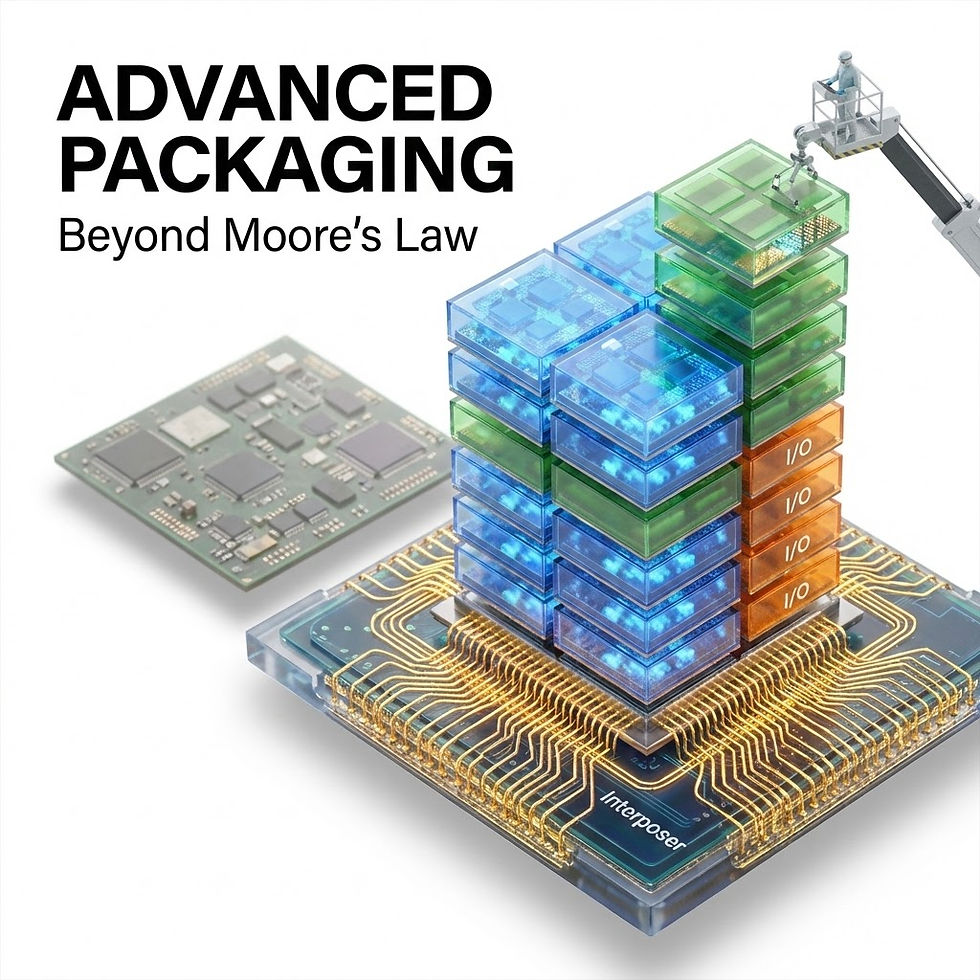
Before contrasting the three CoWoS branches, non-technical readers can unlock the entire architecture by understanding the Four-Layer Nanometer Hierarchy inside a modern AI accelerator package. Asking "Is CoWoS a 2nm or 3nm technology?" is like asking whether a modern airport is made of titanium jet engines or reinforced concrete runways—it purposefully combines both!
Inside a single CoWoS super-package, four distinct technology tiers work in concert:
Tier 1 — The Penthouse Compute Brains (7nm → 5nm/4nm → 3nm N3E/N3P → 2nm N2 & 1.6nm A16): The active GPU, CPU, or custom AI XPU chiplets on top utilize the world's smallest, most expensive EUV transistors to maximize compute density and energy efficiency.
Tier 2 — The Adjacent HBM Skyscrapers & Logic Lobbies (Specialty DRAM + 12nm/5nm Base Dies): Stacked memory dies store model weights, while HBM4 base dies sitting at the bottom of each memory tower transition onto TSMC's 12nm or 5nm foundry logic nodes to manage massive 2,048-bit traffic flows.
Tier 3 — The CoWoS Interposer Plaza (65nm/45nm Mature Silicon CMOS or 2µm Polymer RDL): This middle layer is the heart of CoWoS! Because an interposer primarily routes microscopic copper highways and stabilizes power—rather than switching billions of logic gates—any silicon used in this layer is fabricated on mature, fully depreciated 65nm (or 40nm/45nm-class) wafer tools. Crucially, mature-node fabs embed Deep Trench Capacitors (eDTC) directly into the silicon interposer, acting like microscopic underground water reservoirs right beneath the GPU to prevent voltage droops when billions of transistors fire simultaneously. (Notably, 65nm wafers still contributed a rock-steady 4% of TSMC's total USD 46.7 billion Q3 2026 revenue, bolstered heavily by interposers and specialty silicon!)
Tier 4 — The Structural Package Substrate (20-Layer ABF Organic or Future Glass Core): Fans out connections from the interposer's ~100-micron bumps to the motherboard.
With that four-tier mental map established, the difference between CoWoS-S, CoWoS-R, and CoWoS-L comes down entirely to how Tier 3—the Interposer Plaza—is constructed. Think of them as three distinct civil-engineering strategies for building the foundation plaza of a futuristic megacity:
1. CoWoS-S (Silicon Interposer) — "The Solid Italian Marble Plaza"
How It Works & Analogy: The suffix "-S" stands for Silicon. Engineers carve the entire foundation plaza out of a single, unbroken monolithic slab of 65nm-class silicon pierced by tens of thousands of vertical copper elevators called Through-Silicon Vias (TSVs). Because the marble plaza is made of the exact same pure silicon material as the GPU skyscrapers sitting on top of it, there is near-zero thermal expansion mismatch at the top interface, and wafer steppers can etch ultra-dense sub-micron copper wiring (<0.5 µm line/space) uniformly from edge to edge.
Strengths & Ceiling: Highest uniform wiring density across the entire floor, rock-solid electrical decoupling, and over fourteen years of battle-tested production maturity since 2012. However, monolithic marble slabs hit a hard economic and fracture ceiling around 3.3× reticle size (~2,700 mm², accommodating roughly up to 8 HBM stacks).
Process Node Pairings & Flagship Silicon: Primarily paired with 7nm (N7), 5nm/4nm (N5/N4P), and compact 3nm designs whose total silicon envelope fits comfortably inside 3.3× reticle. Iconic deployments include NVIDIA's A100 (7nm) and Hopper H100 / H200 (4nm), AMD's Instinct MI300X, MI325X, and CDNA 4 MI350 / MI355X accelerators (which stack 5nm or 3nm compute chiplets onto 6nm active I/O base dies atop a CoWoS-S silicon interposer), Google's TPU v5p / v6e, and ultra-high-end FPGAs.
Strategic Niche: The gold-standard turnkey platform for single-die or compact multi-chiplet AI accelerators requiring maximum uniform signal density within a ≤2,700 mm² footprint.
2. CoWoS-R (RDL Organic Interposer) — "The Flexible Shock-Absorbing Asphalt Expressway"
How It Works & Analogy: Entering volume production in 2023, the suffix "-R" stands for Redistribution Layer (RDL). CoWoS-R throws away the expensive monolithic silicon wafer slab and eliminates TSV silicon drilling altogether! Instead, engineers build the plaza out of six or more alternating layers of flexible organic polymer film and fine copper traces (achieving a 4-micron minimum pitch with 2-micron line width and spacing), while tucking tiny discrete silicon Integrated Passive Devices (IPDs) into noisy pockets near HBM rings to keep power clean. Think of replacing brittle marble with a multi-deck, flexible polymer-asphalt highway system that bends gracefully without cracking.
Strengths & Trade-offs: Lowest manufacturing cost in the CoWoS family and superior mechanical compliance. Because polymer films flex smoothly, CoWoS-R acts as a mechanical stress buffer between silicon dies on top and 20-layer ABF substrates underneath, delivering exceptional solder-joint reliability across large footprints. The trade-off is wiring density: 2-micron polymer lines cannot match sub-micron silicon lines for stitching two massive GPUs together at 10 Terabytes per second, yet they easily provide the tens-of-microns micro-bump density required to connect an AI ASIC to multiple HBM3E stacks or chip-to-chip links.
Process Node Pairings & Flagship Silicon: Pairs seamlessly with 7nm (N7), 5nm (N5), and cutting-edge 3nm (N3E/N3P) custom cloud silicon and high-radix networking switches where Total Cost of Ownership (TCO) and rapid manufacturing cycle times dictate architecture! The premier flagship showcase for CoWoS-R is Amazon Web Services (AWS): spanning Inferentia2 (7nm), Trainium2 (5nm N5), and AWS's 2026 powerhouse Trainium3—one of the industry's very first server accelerators built on TSMC's 3nm N3P node paired with 12-high HBM3E (9.6 Gbps pin speed) atop a 6-layer RDL CoWoS-R interposer! High-bandwidth data-center Ethernet switch ASICs (Broadcom/Marvell class), 5G infrastructure, and automotive super-SoCs similarly leverage CoWoS-R.
Strategic Niche: The undisputed TCO & Scale-Out Efficiency Champion for hyperscaler custom AI ASICs (XPUs) and networking silicon that need HBM bandwidth and large package footprints without paying for a full sheet of silicon.
3. CoWoS-L (RDL + Local Silicon Interconnect) — "The Hybrid Aircraft Carrier with Localized Diamond Skybridges"
How It Works & Analogy: Entering 3.5× reticle volume in 2024 and ramping 5.5× reticle volume in 2026, the suffix "-L" stands for Local Silicon Interconnect (LSI). CoWoS-L marries the best physics of both siblings: roughly 80% of the interposer body is molded from flexible, crack-resistant polymer RDL (coupled with vertical copper pillars called Through-InFO Vias, or TIVs, for clean power delivery), while tiny, pre-fabricated 65nm-class Local Silicon Interconnect (LSI) bridges are surgically embedded only directly beneath the borders where two compute dies abut or where compute dies interface with HBM stacks! Imagine building a sprawling ten-block metropolis on resilient polymer ground to prevent earthquakes from cracking the foundation, while erecting ultra-dense, sub-micron solid-silicon skybridges exclusively between adjacent financial skyscrapers that exchange terabytes of data every second.
Strengths & Scaling Roadmap: Obliterates the 3.3× reticle ceiling while preserving pure-silicon wiring density at critical interfaces—at a unit cost positioned squarely between CoWoS-S and CoWoS-R! Having achieved >98% interposer yields on 5.5× reticle (~4,700 mm²) in 2026, TSMC's official roadmap scales CoWoS-L to 9× / 9.5× reticle (>7,700 mm², 12+ HBM4 stacks) in 2027 and an astonishing 14× reticle by 2028—engineered to unite roughly 10 full-sized compute dies and 20 HBM stacks on a single package!
Process Node Pairings & Flagship Silicon: The mandatory launchpad for 4nm (N4P), 3nm (N3E/N3P), 2nm (N2), and 1.6nm (A16) multi-reticle frontier AI superchips! Commercial anchors include NVIDIA's entire Blackwell lineup (B200 / GB200 / B300 on 4nm N4P), NVIDIA's Vera Rubin architecture (3nm N3P compute dies + HBM4 on 5.5× CoWoS-L ramping from late 2026 into 2027), AMD's Instinct MI400 / MI450 generation and 6th-Gen EPYC "Venice" server CPUs (stacking 2nm N2 and 3nm N3P active chiplets via 3D SoIC hybrid bonding on top of CoWoS-L), and top-tier frontier training XPUs.
Strategic Niche: The Undisputed Flagship Workhorse of Global AI Infrastructure through 2030, capturing the vast majority of TSMC's incremental capacity additions.
Why Is This Revolutionary?
Splitting CoWoS into specialized -S, -R, and -L platforms unlocks three structural breakthroughs that sustain AI compute scaling well beyond traditional transistor shrinking:
Decoupling Silicon Die Yield from System Compute Scale: Fabricating two medium-sized 3nm or 2nm compute dies and stitching them across an LSI bridge inside CoWoS-L delivers dramatically higher wafer yields than attempting an impossible monolithic chip, while maintaining a blistering 10 TB/s coherent die-to-die link that makes multiple chiplets behave software-identically to a single gigantic processor.
Architectural Segmentation Across the Hyperscaler CapEx Stack: Not every AI workload requires a $40,000 dual-reticle liquid-cooled monster. By offering CoWoS-R alongside CoWoS-L, TSMC empowers cloud providers like AWS to optimize tokens-per-dollar-per-watt across air-cooled and liquid-cooled data centers on 3nm N3P (Trainium3), while simultaneously enabling NVIDIA and AMD to push multi-kilowatt frontier training boundaries (up to 2,000W–4,100W package thermal envelopes) on CoWoS-L.
Enabling Vertical 3D + 2.5D Convergence ("SoIC-on-CoWoS"):Starting aggressively in late 2026 and 2027 with 2nm (N2) architectures like AMD's MI400 series, chipmakers are stacking 2nm compute chiplets directly atop 3nm active base dies using bump-less copper-to-copper SoIC (System-on-Integrated-Chips), and then mounting multiple 3D-stacked towers plus HBM4 cubes onto a giant CoWoS-L base—turning chip packaging into three-dimensional modular skyscrapers.
Industry Impact and Competitive Landscape
Who Are the Key Players?
Fueled by $725 billion in 2026 hyperscaler capital expenditures (+77% YoY) and projections for another 30% to 40% expansion in 2027, the CoWoS value chain has triggered historic alliances across foundries, Outsourced Semiconductor Assembly and Test (OSAT) giants, specialty substrate makers, and precision equipment monopolists:
1. The Ecosystem Architect: TSMC (NYSE: TSM / TWSE: 2330)
Commanding roughly 92% share of leading-edge AI logic wafers and owning the CoWoS standard, TSMC is executing the fastest advanced-packaging buildout in semiconductor history. Alongside Fab AP6 in Zhunan, TSMC converted acquired flat-panel cleanrooms in Tainan (AP8) and brought Chiayi AP7 Phase 1 into mass production in June 2026, lifting internal CoWoS capacity past 130,000 wafers per month by year-end 2026 on the march toward ~200,000 wpm in 2027 and ~260,000 wpm by end-2028. NVIDIA alone commands well over 50% of total CoWoS allocation, followed by Broadcom (powering Google TPU and Meta custom silicon), AMD, AWS/Marvell/Alchip, and MediaTek.
2. The Geopolitical Surprise Partner: GlobalFoundries (NASDAQ: GFS)
On October 8, 2026, GlobalFoundries stunned Wall Street by signing a multi-year, USD 2 billion manufacturing agreement with TSMC to establish the first US-based supply of CoWoS silicon interposers (incorporating embedded deep trench capacitors) at GF's Fab 8 in Malta, New York, ramping volume in H1 2028. The industrial logic is surgical: silicon interposers and LSI components require mature 45nm/65nm lithography, 10-micron TSV etching, and deep-trench eDRAM-style capacitors—capabilities GF Malta already excels at without needing a single EUV scanner. Offloading mature silicon interposers to New York frees TSMC's cleanrooms for high-margin N2/A16 wafers and CoWoS-L assembly while satisfying US CHIPS Act domestic supply-chain mandates alongside TSMC's Arizona logic fabs.
3. The OSAT Margin Revolution: ASE Technology Holding (NYSE: ASX) & Amkor Technology (NASDAQ: AMKR)
Because demand persistently outstrips TSMC's internal back-end cleanrooms by 20%+, TSMC systematically outsources overflow WoS (Wafer-on-Substrate) final assembly as well as full-flow 2.5D equivalents for CoWoS-S and CoWoS-R designs.The financial impact materialized dramatically during ASE Technology Holding's October 29, 2026 Q3 earnings call: ASE's packaging and test (ATM) gross margin vaulted 800 basis points year-over-year to 30.6%, shattering historical OSAT margin ceilings! Management hiked 2026 CapEx to USD 11.5 billion and raised 2026 LEAP (Leading-edge Assembly and Packaging) revenue guidance above USD 4 billion—projecting LEAP revenue to double again in 2027 toward USD 8 billion! Simultaneously in the United States, Amkor Technology is building out the first US outsourced CoWoS-L-class advanced packaging facility in Peoria, Arizona under TSMC technology partnership, securing key spillover allocations including AMD server processors and hyperscaler accelerators.
4. Precision Packaging Equipment, Metrology & Test Tollbooths
Transitioning from CoWoS-S to multi-reticle CoWoS-L multiplies process steps—requiring sub-micron LSI die-attach, polymer RDL lamination, molded underfill, wafer thinning, and 100% optical inspection:
Global Equipment & Metrology Leaders: Besi (BE Semiconductor) and ASMPT dominate ultra-high-accuracy thermo-compression and hybrid die bonding; Applied Materials and Lam Research control TSV deep silicon etching, copper electroplating, and CMP planarization; Onto Innovation, KLA, and Camtek capture booming metrology demand for inspecting micro-bumps, RDL trace defects, and LSI alignment; SUSS MicroTec and EV Group (EVG) supply temporary carrier wafer bonders/debonders critical for handling fragile reconstructed wafers.
Specialized Asian Equipment & High-Power Test Champions: Taiwan's wet-bench/cleaning duopoly Grand Process Technology (3131.TW) and Scientech (3583.TW), precision die-sorter/dispenser specialists Gallant Micro. Machining (6640.TW) and Allring Tech (6187.TW), and RDL vacuum lamination leader C Sun Mfg (2467.TW) operate at full order visibility into 2027. Downstream, testing $30,000+ multi-chiplet assemblies drives secular booms for Advantest, Teradyne, final-test powerhouse KYEC (2449.TW), MEMS probe-card/socket leaders FormFactor, MPI (6223.TW), and WinWay (6515.TW), and high-layer-count ABF substrate titans Ibiden and Unimicron (3037.TW).
Adoption Timeline and Challenges
Tracking TSMC symposium disclosures and supply-chain qualification milestones establishes a clear multi-year roadmap:
2026 (The 5.5× CoWoS-L & 3nm N3P Inflection): 3.5× CoWoS-L ships in massive volume (Blackwell), 5.5× CoWoS-L enters commercial production at >98% interposer yield (supporting NVIDIA Vera Rubin ramps), CoWoS-R scales on 3nm N3P (AWS Trainium3), and TSMC's Chiayi AP7 Phase 1 comes online.
2027 (9× / 9.5× Reticle Super-Packages & 16-High HBM4): CoWoS-L expands past 7,700 mm² to host 12+ HBM4 stacks alongside 2nm (N2) + SoIC 3D-stacked compute tiles, while total TSMC + OSAT monthly capacity pushes past 200,000 wafers.
2028–2029 (14× Reticle Megastructures, US Interposers & Panelization): TSMC targets 14× reticle CoWoS-L (~10 large compute dies + 20 HBM stacks), GlobalFoundries Malta NY begins shipping US-made silicon interposers, Amkor Arizona scales US back-end assembly, and rectangular CoPoS (Chip-on-Panel-on-Substrate) enters commercial high-volume manufacturing.
Four major engineering realities explain why supply remains tight despite record CapEx:
The "Wafer Arithmetic Distortion" Trap (Why Wafers Per Month Overstates Actual Chip Supply): Investors frequently model CoWoS supply simply by looking at TSMC's headline "wafers per month (wpm)" figure. Yet CoWoS is built on round 300mm carrier wafers (~70,685 mm² surface area). When interposers measured 1.5× to 2× reticle, one wafer yielded 25 to 30 packages. At 5.5× reticle (~4,700 mm²) for Vera Rubin, geometric circle-packing dictates that a single 300mm wafer yields ONLY 7 usable packages—leaving 55% of the round wafer unused around the curved edges! Moving to 9.5× reticle in 2027 cuts yield per wafer down to just 3 or 4 packages! Consequently, doubling wafer capacity from 65,000 to 130,000 wpm does not double finished GPU output when package sizes simultaneously double—explaining structurally why packaging shortages persist into 2027–2028.
Reconstructed Wafer Warpage and Carrier Debonding:CoWoS-L involves molding tiny LSI silicon chips inside liquid epoxy compound to create a "reconstructed wafer," grinding it thin, patterning fine RDL copper layers, attaching massive GPUs and tall 16-high HBM4 cubes, and detaching glass carrier wafers—all without letting differential thermal expansion bend the assembly by more than microns.
Simultaneous Switching Noise (SI/PI) at 4,000+ Watts: Delivering clean sub-1V power across thousands of amperes while 24,000+ HBM4 data lanes switch at 8–10 GT/s pushes signal and power integrity (SI/PI) to physical limits, requiring intricate co-design of eDTC silicon capacitors and low-loss RDL shielding.
Known-Good-Die (KGD) Scrap Economics: Because a 5.5× or 9.5× CoWoS-L module binds together tens of thousands of dollars of 3nm/2nm logic and scarce HBM4 memory, even a 1% late-stage assembly defect rate inflicts severe dollar scrap penalties.
Potential Risks and Alternatives
Objective investors must track four competitive and architectural counter-currents:
1. Intel Foundry's EMIB / EMIB-T & Samsung's I-Cube:
Architecturally, Intel's EMIB (Embedded Multi-die Interconnect Bridge) pioneered the concept of embedding small silicon bridges directly into rectangular organic package substrates—avoiding round-wafer area waste. Intel is actively pitching EMIB-T (adding TSVs to its bridges for HBM4 power delivery) as an available capacity valve for AI ASIC designers frustrated by TSMC queues. Still, because hyperscalers overwhelmingly prefer keeping 3nm/2nm wafer fabrication and advanced packaging under a single accountable roof (TSMC's "one-stop shop"), CoWoS retains commanding market share.
2. Rumored "CoWoP" (Chip-on-Wafer-on-PCB) Substrate-Less Experiments:
Supply-chain leaks in 2026 sparked debate around CoWoP—an experimental concept proposing to eliminate the ABF package substrate entirely and mount the CoW interposer assembly directly onto an ultra-high-density server motherboard PCB to trim substrate loss and improve top-side cooling. However, institutional hardware analysts (including Morgan Stanley) note that bridging micron-scale interposer bumps directly onto massive, thermally expanding server motherboards introduces daunting yield and serviceability risks, making near-term displacement of CoWoS + ABF substrates on flagship GPUs highly unlikely.
3. Rectangular Panelization (FOPLP / CoPoS) and Exotic Interposer Materials:
To solve the "7 packages per round wafer" geometric penalty permanently, both TSMC (CoPoS, targeted for 2028–2029) and OSATs (ASE FOEB/VIPack, Innolux) are racing to migrate RDL+bridge flows onto large square/rectangular panels (e.g., 300×300mm or 510×515mm), alongside early R&D into ultra-conductive Silicon Carbide (SiC) interposers for multi-kilowatt thermal dissipation. While bullish for long-term AI scaling, rectangular panel transitions will eventually require re-tooling 300mm round-wafer equipment lines.
4. Custom ASIC Shift Toward Lower-Cost CoWoS-R:
With custom cloud XPUs projected to capture 30% to 40% of AI compute CapEx by 2028, if more cost-driven inference chips opt for CoWoS-R (like AWS Trainium3) rather than silicon-bridge CoWoS-L, revenue mix within packaging material suppliers will tilt further toward polymer RDL chemistries and IPDs rather than monolithic silicon wafers.
Future Outlook and Investor Perspective
Stepping back to view the semiconductor value chain from 30,000 feet, TSMC's segmentation of CoWoS into -S, -R, and -L represents a masterclass in technological moat-building. Rather than leaving a price-umbrella opening for rivals at the cost-sensitive end or hitting a physical fracture ceiling at the ultra-high end, TSMC bracketed the entire market: CoWoS-R locks in TCO-focused 3nm cloud ASICs and networking switches; CoWoS-S monetizes mature 4nm/5nm accelerators; and CoWoS-L (paired vertically with 3D SoIC) establishes an unassailable fortress around 3nm, 2nm, and A16 multi-reticle frontier AI supercomputers.
For global equity investors positioning portfolios for 2026 through 2030, four high-conviction takeaways stand out:
1. Discount "Wafer" Headline Growth—Own the "Package Area Inflation" Equipment Winners: Because migrating from 3.3× CoWoS-S to 5.5× and 9.5× CoWoS-L slashes the number of finished chips harvested per 300mm wafer down to single digits, wafer-level packaging tool intensity per GPU shipped is structurally rising! Precision die-bonding, RDL lithography/lamination, wet-etch cleaning, and optical metrology suppliers (Besi, Applied Materials, Onto Innovation, KLA, Camtek, SUSS MicroTec, alongside Taiwanese leaders Grand Process, Scientech, Allring, and Gallant Micro) enjoy multi-year demand visibility decoupled from unit smartphone or PC cycles.
2. Capture the Structural OSAT Gross-Margin Re-Rating:ASE Technology Holding's breakthrough to 30.6% ATM gross margins and a USD 4B+ LEAP revenue run-rate (set to double in 2027) alongside Amkor's US Arizona CoWoS-L expansion proves that top-tier OSATs are no longer low-margin wire-bonding shops—they have become indispensable, capital-protected extensions of TSMC's AI back-end fabs.
3. Play Both Sides of the AI Compute Split (GPU CoWoS-L vs. Cloud XPU CoWoS-R): Rather than betting exclusively on whether merchant GPUs (NVIDIA, AMD) or hyperscaler custom ASICs (Broadcom, Marvell, AWS, Google) win market share, owning TSMC, custom ASIC design houses, high-layer-count ABF substrate oligopolists (Ibiden, Unimicron), and high-power burn-in/SLT test leaders (Advantest, Teradyne, FormFactor, KYEC) taxes every single CoWoS-L and CoWoS-R package leaving the cleanroom.
4. Watch Mature Specialty Foundries Repurposed for AI Packaging: GlobalFoundries' USD 2 billion CoWoS interposer pact demonstrates that mature 45nm/65nm fabs equipped with TSV and deep-trench capacitor capabilities hold hidden strategic value as sovereign AI packaging enablers in North America and Europe.
In the Post-Moore's Law era, transistor nanometer numbers grab the headlines, but microscopic copper bridges and polymer plazas dictate who actually ships intelligence at scale. Investors who understand the distinct mechanics and economics of CoWoS-S, CoWoS-R, and CoWoS-L hold the blueprint to the single most durable profit pool in modern hardware.

