Advanced Packaging & CoWoS: The Life Support for Moore's Law and the New Foundry Battlefield
- Feb 11
- 4 min read
Key Takeaway: Why You Need to Understand This Now
For the past 50 years, the rule of the semiconductor game was simple: shrink the transistor (e.g., from 7nm to 3nm). But now, that road has hit a wall. Physics tells us we can't split atoms infinitely, and smaller chips are becoming exponentially more expensive with lower yields.
However, AI's hunger for computing power is bottomless. Since we can't make "single chips" much bigger or faster using old methods, engineers came up with a brute-force solution: "Stitch different chips together like Lego blocks, or even stack them."
This is the core concept of Advanced Packaging, and the essence of TSMC's CoWoS (Chip on Wafer on Substrate) technology. The investment logic has shifted: whoever can "package" the chips best is the new king. This blurs the line between traditional assembly houses (OSATs) and foundries, creating massive opportunities for new equipment supply chains (like wet processing, bonders, and metrology). Simply put, packaging is no longer just "wrapping paper"; it is now part of the "brain's neural network."
Tech in Plain English: Core Principles and Breakthroughs
To understand Advanced Packaging, we must distinguish between the "Front-end" (making the chip) and the "Back-end" (packaging the chip).
The Past Bottleneck: What Problem Does It Solve?
Reticle Limit: Lithography machines can only expose a fixed maximum area. AI chips want to cram in more transistors, but the physical size cannot exceed this limit.
The Curse of Yield: The larger the chip, the higher the probability of a defect. If you make one massive chip, a single speck of dust ruins the whole thing (huge cost). If you chop it into four small chips, you only throw away the broken piece.
The Memory Wall: Memory (DRAM) is often too far from the computing core (GPU). Data moves too slowly across the circuit board, starving the processor.

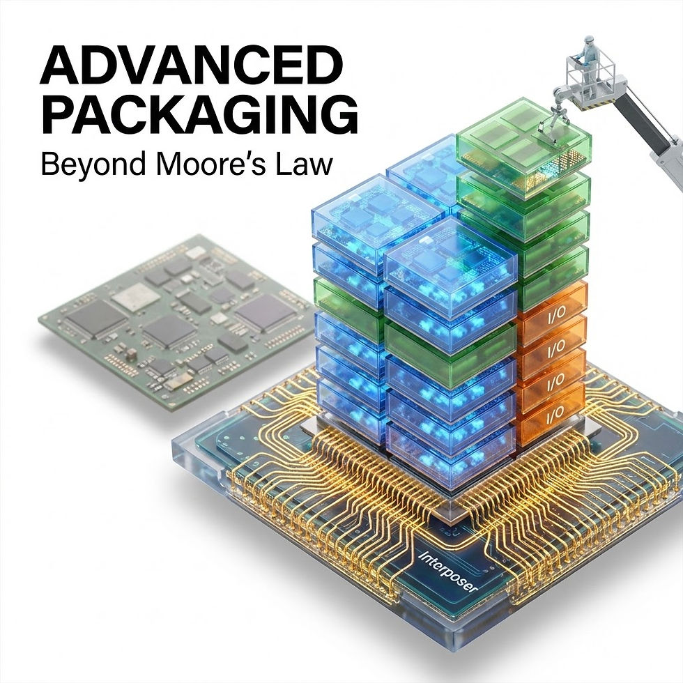
How Does It Work? (Lego Blocks and Skyscrapers)
Advanced Packaging (specifically 2.5D and 3D IC) can be explained using "Urban Planning":
1. Traditional Packaging (2D) — Suburban Houses Chips are like houses scattered in the suburbs, separated by long roads (the PCB). For data to travel from House A to House B, it must drive along these long roads—slow and gas-guzzling (energy inefficient).
2. CoWoS (2.5D Packaging) — The Superhighway The key to CoWoS is something called the "Interposer."
Mechanism: Instead of placing chips on the PCB, we place them side-by-side on a special silicon basement (the Interposer). Buried inside this basement are thousands of microscopic "fiber-optic-like" cables.
Effect: The GPU (Brain) and HBM (High Bandwidth Memory) move into the same gated community, connected by dedicated underground tunnels. Data transfer speeds skyrocket.
3. 3D IC (SoIC) — The Skyscraper This is even more radical. We stack chips directly on top of chips. Like building a skyscraper, elevators (TSV - Through-Silicon Vias) run vertically through the floors. The distance is shortest, speed is fastest, but heat management is the hardest.

Why Is This Revolutionary? (The Chiplet Era)
This enables the Chiplet business model. Previously, you bought a computer as a single "flagship unit." Now, manufacturers can assemble it like Lego:
Compute Core: Expensive 3nm process.
I/O Controller: Cheaper 12nm process.
Memory: Bought from Micron. Finally, "glue" them together using Advanced Packaging. This drastically reduces design costs (NRE) and improves yield.
Industry Impact and Competitive Landscape
The rise of Advanced Packaging has turned a traditionally low-margin, low-tech industry into a high-tech arms race.
Who Are the Key Players? (Supply Chain Analysis)
Foundries (The Kings):
TSMC: The dominator of CoWoS. Currently, all high-end NVIDIA AI chips must be packaged by TSMC. TSMC is no longer just "making" chips; it is capturing the high-value "packaging" profit.
Intel: Pushing its "Foveros" technology, attempting to leapfrog in the foundry market via packaging superiority.
Equipment Suppliers (The Arms Dealers):
Besi (Netherlands): The leader in Hybrid Bonding, the technology needed to glue chips with extreme precision (<1 micron accuracy).
Disco (Japan): The absolute king of "Dicing and Grinding." As chips get stacked, wafers must be ground ultra-thin and cut with laser precision.
Camtek / KLA: Metrology and Inspection. With thousands of connections, you need eyes that can see defects at the atomic level.
OSATs (The Assembly Houses):
ASE: While TSMC takes the ultra-high-end CoWoS, ASE dominates the mid-to-high-end (Fan-out) market. As technology trickles down, OSATs will capture high volumes of consumer AI chips.

Adoption Timeline and Challenges
Now: Extreme shortage. The 52-week lead time for NVIDIA H100s is primarily due to the CoWoS bottleneck, not the GPU die itself.
Future Challenge: Heat Dissipation. When you stack chips like a sandwich, the heat in the middle layer gets trapped. This links back to the importance of "Liquid Cooling" discussed in our previous article.
Potential Risks and Alternatives
Glass Substrates: Intel is aggressively pushing to replace current organic/silicon interposers with Glass. Glass is flatter, stiffer, and allows for finer holes. If successful, this could disrupt the entire materials supply chain.
Future Outlook and Investment Perspective
Advanced Packaging signals the official arrival of the "Post-Moore's Law Era."
From an investment perspective, watch the shift in "Value Content":
CapEx Explosion: The percentage of Foundry CAPEX dedicated to "Back-end" is at historical highs. Buying equipment suppliers (like Besi, Disco, or local champions in Taiwan) has been the winning strategy, and the focus is now moving to "Metrology" and "Bonding."
Yield is Margin: Advanced packaging yields are still lower than front-end processes. Whoever provides solutions to boost yield (like AI-powered AOI inspection) commands a premium.
Ecosystem Lock-in: In the Chiplet era, chip designers will rely more heavily on the packaging ecosystem (like the UCIe standard).
The future chip war isn't just about who has the smallest nanometer number, but who can stack the tallest, most stable Lego tower.
If this "Lego Science of Chips" helped you understand Advanced Packaging, could you please share or hit Like? Your small encouragement is the biggest motivation for this little station to keep decoding hard-core tech for you! Thank you!


Comments