Trading Electrons for Photons: Decoding Silicon Photonics and CPO, the Ultimate Interconnect for AI's Data-Hungry Future
- Oct 19, 2025
- 7 min read
Why You Need to Understand This Now
We've established that AI's prowess comes from powerful GPU "brains" and the high-bandwidth memory (HBM) "hearts" that sustain them. But a new, colossal problem is emerging: when you assemble thousands of these brain-heart units into a massive AI factory (a data center), how do you get them to talk to each other without creating a system-wide traffic jam?
The traditional method uses copper wires. But as AI workloads have exploded, the sheer volume of data is causing these copper lanes to "choke." It's like trying to manage Formula 1 race traffic using narrow city streets—the result is gridlock, immense heat (power consumption), and a hard ceiling on speed. It doesn't matter how fast your AI processor can think if the data it needs is stuck in traffic.
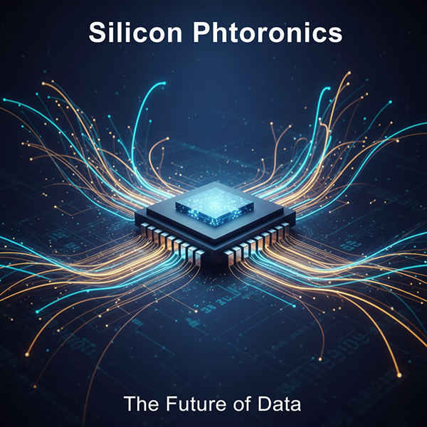
Silicon Photonics is the elegant, revolutionary solution to this crisis. Its core concept is simple yet profound: transmit data using light instead of electricity. It achieves this by fabricating microscopic versions of optical components—lasers, modulators, waveguides—directly onto a silicon chip, creating a light-speed network on a chip. Co-Packaged Optics (CPO) takes this a step further by integrating this "optical engine" directly alongside the main processing chips (like GPUs or switches) within the same package, creating a seamless, ultra-high-bandwidth connection.
In short, Silicon Photonics with CPO is building a private, zero-latency wormhole for AI data. The maturation of this technology will directly determine whether AI can break through its current scaling barriers to achieve true, hyperscale intelligence. This is precisely why tech titans like TSMC, Intel, Broadcom, and NVIDIA are in an all-out race to dominate this next frontier.

The Technology Explained: Principles and Breakthroughs
The Old Bottleneck: What Problem Does It Solve?
In a large AI data center, massive amounts of data flow between network switches (the traffic cops) and servers (the compute units). For decades, this has been handled by pluggable optical modules, but this architecture has a fatal flaw:
The "last mile" for the electrical signal is far too long.
Specifically, data originating from a GPU travels as an electrical signal across several inches of copper traces on a printed circuit board (PCB). Only when it reaches the edge of the server box does it get plugged into an optical module, which finally converts the electrical signal into a light signal to be sent over fiber optics. This journey creates three massive problems:
Massive Power Consumption: Pushing high-speed electrical signals through copper is like running against a strong wind; resistance causes significant energy loss, which dissipates as waste heat. In modern data centers, I/O (input/output) connectivity accounts for a shockingly large portion of the total power bill.
Signal Degradation: The faster you push the electrical signal, the more it degrades over distance. Maintaining signal integrity requires complex and costly retimers and amplifiers on the board, adding expense and complexity.
Limited Bandwidth Density: There's a physical limit to how many copper traces you can cram around a chip. This "shoreline density" problem puts a hard cap on a chip's total ability to communicate with the outside world.
The goal of CPO is to completely eliminate this inefficient, power-hungry electrical last mile.
How Does It Work? (The Power of Analogy)
Imagine you are designing a brand-new logistics system for a megacity (an AI chip).
The Old Way (Pluggable Optics): This is like forcing all the city's goods (data) to be loaded onto gas-guzzling trucks (electrical signals). These trucks must navigate congested, inefficient city streets (the PCB traces) to reach a seaport at the city's edge (the pluggable module). Only there can the goods be loaded onto massive container ships (optical signals) for long-haul transport. The process is slow, polluting (high power consumption), and expensive.
The New Way (Co-Packaged Optics): This is a radical redesign. You build a deep-water port (the silicon photonics engine) right in the city center, directly adjacent to the main business district (the GPU).
The Silicon Photonics Engine: Using standard semiconductor manufacturing, scientists "carve" all the necessary optical components onto a silicon chip. This is like building a miniature, fully-functional port with its own laser lighthouses (light source), signal modulation docks (modulators), waveguide channels (waveguides), and cargo inspection stations (photodetectors).
Electrical-to-Optical Conversion: When the GPU has a batch of goods (an electrical signal) to send, it no longer needs the trucks. It sends the data directly to the adjacent "modulation dock." This dock instantly translates the electrical "0s" and "1s" into pulses of light—"on" and "off"—effectively loading the cargo onto the ship.
Co-Packaging: The critical step. Using advanced packaging, this miniature port is placed shoulder-to-shoulder with the city's CPU/GPU on the same foundation (substrate). The distance between them is microscopic.
Direct Fiber Connection: Once loaded, the "ship" of light sails down a fiber optic cable—a frictionless superhighway of the sea—at light speed, with virtually no energy loss.
Why Is This a Revolution?
CPO is revolutionary because it fundamentally re-architects how a chip communicates, leading to dramatic, systemic gains.
Drastic Power Reduction: By eliminating the most power-hungry part of the signal path—from the chip to the board edge—CPO can reduce I/O power consumption by 30% or more. Across an entire data center, this translates into millions of dollars in saved electricity costs annually.
Massive Bandwidth Density: Optical fibers are tiny. In the same "shoreline" space around a chip, CPO allows for a much higher density of I/O channels, enabling a multi-fold increase in the chip's total bandwidth. This means AI processors can talk to more neighbors simultaneously, dramatically increasing the efficiency of the entire cluster.
Improved Latency and Cost: While initial adoption costs are high, at scale, a highly integrated silicon photonics solution is projected to be more cost-effective than a system relying on numerous discrete components. The ultra-short connection also means lower data latency.
Industry Impact and Competitive Landscape
Who Are the Key Players?
The CPO race is a convergence of giants from the semiconductor, networking, and cloud computing worlds:
Semiconductor Foundries & IDMs:
Intel: The pioneer and long-time leader in the field of silicon photonics. Its integrated device manufacturing (IDM) advantage allows it to develop and fabricate both logic and photonics chips in-house, offering tightly integrated products.
TSMC: The world's semiconductor manufacturing king is leveraging its advanced process and packaging technologies (like CoWoS) to enter the fray. Its COUPE platform aims to create an ecosystem where fabless companies can easily integrate photonic I/O into their chip designs, posing a massive competitive threat.
GlobalFoundries: Another major foundry with a dedicated silicon photonics platform (GF Fotonix™), serving as a key enabler for many companies in the ecosystem.
Networking & Switch Silicon Vendors:
Broadcom & Marvell: As the dominant players in network switch silicon, both are aggressively integrating CPO into their next-generation products to meet the voracious bandwidth demands of their data center customers.
Hyperscalers & End Users:
NVIDIA: As the architect of AI compute, NVIDIA sees CPO as a critical enabler for scaling its future platforms. It is the single largest potential customer and is likely to design its own CPO-enabled solutions to overcome interconnect bottlenecks.
Google, Meta, AWS: These cloud service providers are the ultimate end-users of CPO. Their purchasing decisions, custom silicon roadmaps, and data center architectures will profoundly shape the direction and adoption rate of the entire market.
Adoption Timeline and Challenges
CPO is currently on the cusp of broad commercial deployment. The industry consensus is that large-scale adoption in AI clusters and network switches will begin in the 2025-2027 timeframe, driven by the move to 800G and 1.6T networking speeds.
Key challenges remain:
Light Source Integration: The best material for lasers (Indium Phosphide, InP) is notoriously difficult to integrate with silicon. Developing a cost-effective and reliable method for attaching or growing lasers onto silicon photonics chips is the holy grail of the industry.
Standardization & Ecosystem: CPO is a multi-disciplinary technology. Success requires a robust ecosystem with standards covering everything from chip design and packaging to optical interfaces and testing.
Reliability & Serviceability: Packaging the optics with the silicon means that if a laser fails, the entire expensive package might need to be replaced. This places extreme demands on the long-term reliability of the optical components.
Potential Risks and Alternatives
The primary short-term risk is that the technology's maturity and cost-reduction curve may not meet market timelines. If CPO deployment hits major snags, the industry might lean on interim, "good enough" solutions like Linear Drive Pluggable Optics (LPO), which offers a compromise on power and cost between traditional modules and full CPO.
Long-term, however, the laws of physics dictate that the trend of "light replacing copper" (photons replacing electrons) for data transfer is irreversible. CPO stands as the most promising and powerful end-game solution on the horizon.
Future Outlook and Investor Perspective
The rise of Silicon Photonics and CPO signifies the dawn of a new era: the deep convergence of the semiconductor and optical communication industries. These are no longer two separate worlds but a single, co-evolving ecosystem.
For investors, this technological shift creates new dimensions for analysis:
A New Battlefield Beyond Moore's Law: As gains from shrinking transistors become harder to achieve, the ability to connect chips together becomes a primary value driver. Companies that own the core CPO technology platforms will hold a strategic linchpin in the future of global computing infrastructure.
A Reshaping of the Value Chain: CPO tightly couples the previously separate supply chains for optical components and silicon chips. This means foundry giants like TSMC can expand their total addressable market from logic and SoCs into the high-value domain of optical I/O.
Focus on Ecosystems and Standard-Bearers: In this cross-industry competition, the ultimate winners will likely be those who can build the strongest partner ecosystems and drive industry standards. Investment opportunities exist not only in the technology leaders but also in the critical suppliers of materials, manufacturing equipment, and testing solutions throughout the new value chain.
The journey from copper to fiber, from electron to photon, is more than a change in medium; it's a fundamental reimagining of computation's future. The battle for CPO supremacy is on, and it will define the performance and economics of the next generation of AI, opening up a bright and luminous future for the semiconductor industry.


Comments